Confocal Subsurface Backscattering Microscopy for Optical Identification of Nanoscale Threading Dislocations in SiC Substrates
Pith reviewed 2026-06-28 05:06 UTC · model grok-4.3
The pith
Confocal subsurface backscattering microscopy detects nanoscale threading dislocations in SiC by enhancing strain-induced scattering while suppressing surface reflections.
A machine-rendered reading of the paper's core claim, the machinery that carries it, and where it could break.
Core claim
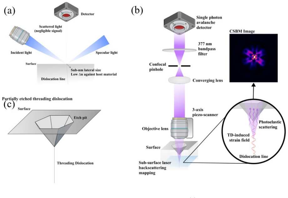
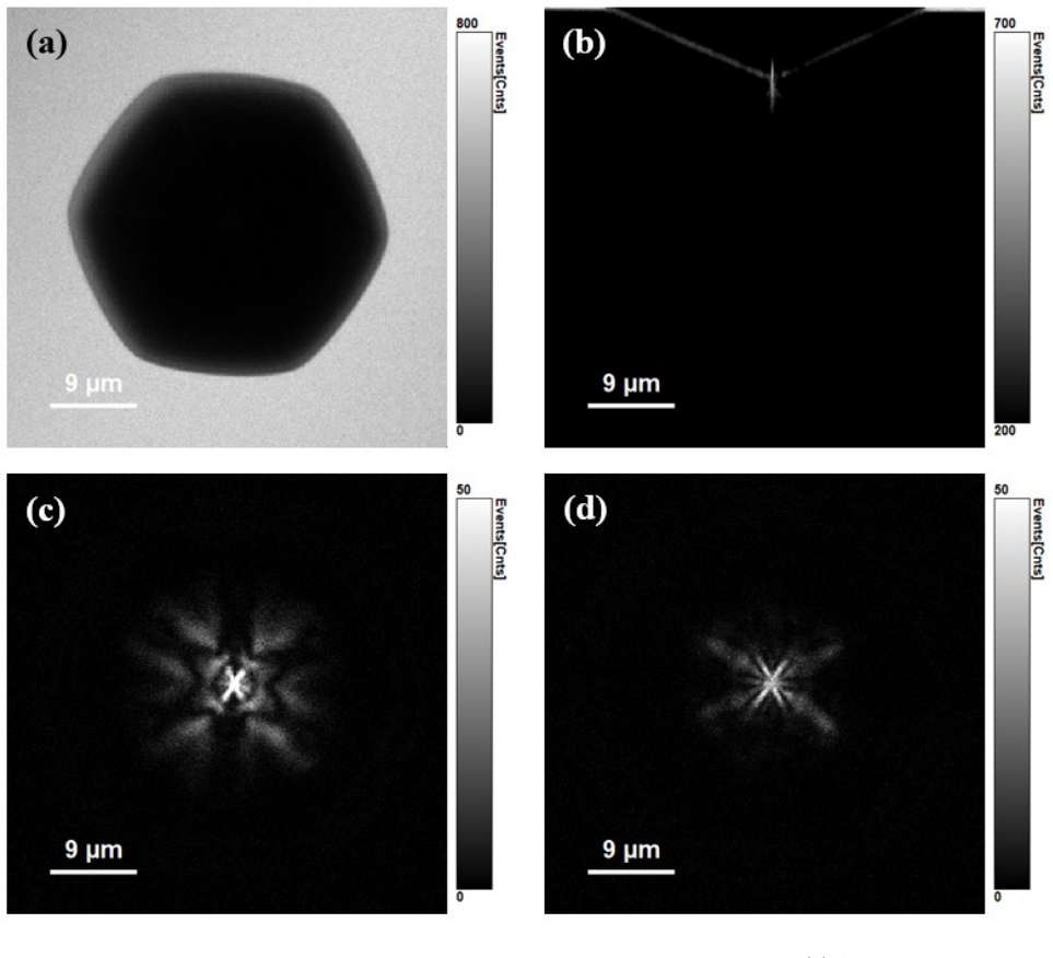
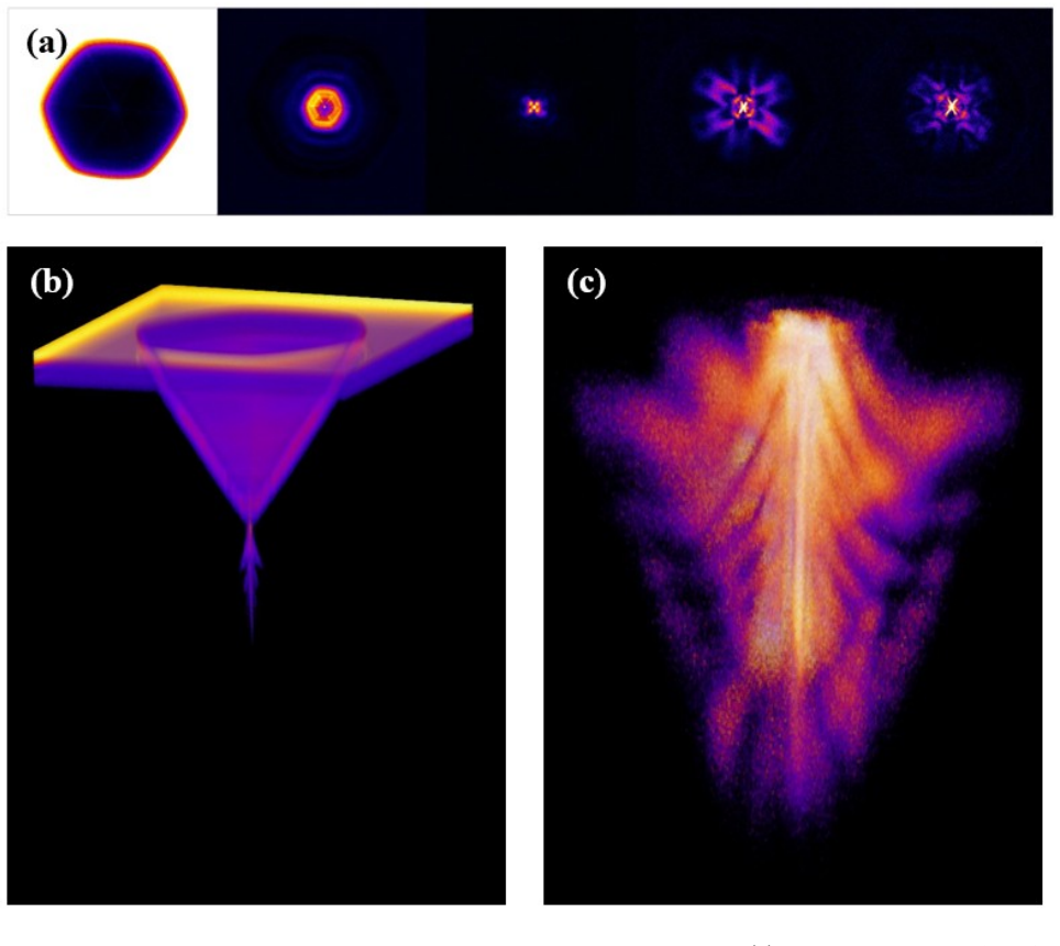
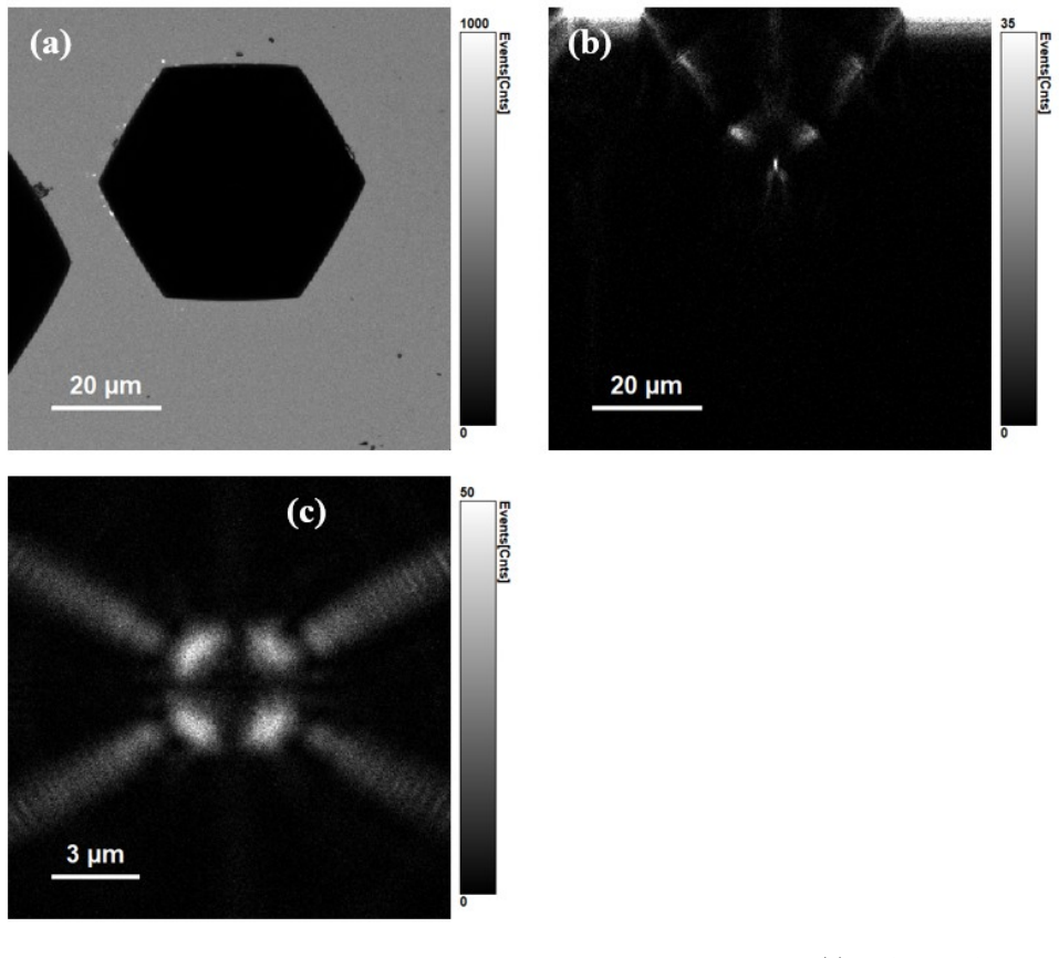
Confocal subsurface backscattering microscopy enables nondestructive detection of nanoscale threading dislocations in SiC substrates based on the synergy of confocal filtering induced dark field configuration and strain induced photoelastic mechanism. By simultaneously suppressing specular reflection while enhancing optical scattering from TD induced refractive index perturbation, CSBM enables high contrast, high resolution TD imaging. Moreover, TD types can be distinguished by their distinct photoelastic scattering patterns.
What carries the argument
Confocal subsurface backscattering microscopy (CSBM), which uses confocal filtering to suppress specular reflection and captures enhanced backscattering from photoelastic refractive-index perturbations induced by threading dislocation strain.
Load-bearing premise
The strain around threading dislocations creates a refractive index perturbation strong enough to produce detectable scattering that stands out after confocal filtering, even without surface features or photoluminescence signals.
What would settle it
Samples containing verified threading dislocations that have been polished to remove surface signatures and doped to quench photoluminescence show no distinct scattering patterns under the CSBM setup.
Figures
read the original abstract
High density threading dislocations in SiC wafers facilitate reverse leakage and degradation, yet commercial defect inspection systems based on surface profiling and PL dark-contrast miss nanoscale TDs because they lack resolvable surface signatures and band-edge PL is uniformly quenched by background dopants or compensating defects. Here, we develop confocal subsurface backscattering microscopy to nondestructively detect TDs, based on the synergy of confocal filtering induced dark field configuration and strain induced photoelastic mechanism. By simultaneously suppressing specular reflection while enhancing optical scattering from TD induced refractive index perturbation, CSBM enables high contrast, high resolution TD imaging. Moreover, TD types can be distinguished by their distinct photoelastic scattering patterns. Our work establishes a simple but effective optical approach for direct TD identification that is more tolerant of surface imperfections, providing a practical route toward industrial in line inspection.
Editorial analysis
A structured set of objections, weighed in public.
Referee Report
Summary. The manuscript introduces confocal subsurface backscattering microscopy (CSBM) for nondestructive detection of nanoscale threading dislocations (TDs) in SiC substrates. It claims that confocal filtering creates a dark-field configuration that suppresses specular reflection while strain-induced photoelastic refractive-index perturbations around TDs produce enhanced, type-specific backscattering contrast, enabling high-contrast, high-resolution imaging even when surface signatures are absent and band-edge photoluminescence is quenched by dopants. The work positions CSBM as a practical, surface-imperfection-tolerant optical method for industrial in-line TD identification and type distinction.
Significance. If experimentally validated, the approach would address a clear gap in commercial SiC wafer inspection by providing an optical, nondestructive alternative to surface profiling and PL methods that fail on doped material lacking resolvable surface features. The potential for type-specific pattern distinction and tolerance to surface imperfections could be valuable for power-electronics quality control.
major comments (1)
- [Abstract] Abstract: the central claims of 'high contrast, high resolution TD imaging' and the ability to 'distinguish TD types by their distinct photoelastic scattering patterns' are stated without any supporting images, quantitative contrast metrics, error analysis, or comparison data in the manuscript. The soundness of the performance assertions therefore cannot be evaluated from the provided text.
Simulated Author's Rebuttal
We thank the referee for their review and the opportunity to address the concern raised. The single major comment focuses on the need for supporting evidence in the manuscript to back the abstract claims; we respond to this point directly below and will revise accordingly.
read point-by-point responses
-
Referee: [Abstract] Abstract: the central claims of 'high contrast, high resolution TD imaging' and the ability to 'distinguish TD types by their distinct photoelastic scattering patterns' are stated without any supporting images, quantitative contrast metrics, error analysis, or comparison data in the manuscript. The soundness of the performance assertions therefore cannot be evaluated from the provided text.
Authors: We agree that the abstract asserts performance characteristics that require explicit substantiation in the main text for the claims to be evaluable. The manuscript as submitted does not include the requested images, quantitative metrics (such as contrast ratios or resolution values), error analysis, or direct comparisons. In the revised version we will incorporate representative CSBM images of TDs, measured contrast values with error bars, statistical analysis of type-specific patterns, and side-by-side comparisons to surface-profiling and PL results on the same samples. These additions will directly support the abstract statements. revision: yes
Circularity Check
No significant circularity; purely qualitative experimental description
full rationale
The paper describes an experimental optical microscopy technique for detecting threading dislocations in SiC via confocal filtering and photoelastic scattering. No equations, derivations, fitted parameters, or self-citation chains appear in the provided text or abstract. The central claim is supported by physical principles of dark-field suppression and strain-induced index perturbation, which are presented as standard mechanisms rather than reduced to the paper's own inputs by construction. The argument is self-contained against external benchmarks with no load-bearing steps that collapse to definitions or prior self-references.
Axiom & Free-Parameter Ledger
Reference graph
Works this paper leans on
-
[2]
et al.Identification and forma- tion mechanism of threading screw dislo- cations in 4H-SiC crystal
Chen, K. et al.Identification and forma- tion mechanism of threading screw dislo- cations in 4H-SiC crystal. Journal of Al- loys and Compounds1040, 183454 (2025). https://doi.org/10.1016/j.jallcom.2025.183454
-
[3]
et al.Relationship between threading dislocation and leakage current in 4H-SiC diodes
Fujiwara, H. et al.Relationship between threading dislocation and leakage current in 4H-SiC diodes. Appl. Phys. Lett.100, 242102 (2012)
2012
-
[4]
Tsuji, T. et al.Analyses of High Leakage Cur- rents in Al+ Implanted 4H SiC pn Diodes Caused by Threading Screw Dislocations. Mater. Sci. Forum645-648, 913-916 (2010). https://doi.org/10.4028/www.scientific.net/MSF.645- 648.913
-
[5]
et al.Impacts of silicon carbide de- fects on electrical characteristics of SiC de- vices
Lai, L. et al.Impacts of silicon carbide de- fects on electrical characteristics of SiC de- vices. J. Appl. Phys.137, 060701 (2025). https://doi.org/10.1063/5.0239362
-
[6]
Cheng, Z. et al.Effect of dopants and surface ox- ides on the electronic properties of dislocations in p-type SiC. Journal of Physics D: Applied Physics 58, 115101 (2025). https://doi.org/10.1088/1361- 6463/ada6d2
-
[7]
Kurniawan, I. S. et al.Nondestructive de- tection and identification of electrically ac- tive threading dislocations in n+-SiC sub- strates. Nanoscale Advances8, 331-339 (2026). https://doi.org/10.1039/D5NA00970G
-
[8]
Kato, M., Sato, H., Kato, T., Murata, K. & Harada, S.Focused light birefringence for three- dimensional observation of dislocations in sili- con carbide wafers. Rev Sci Instrum96, 083901 (2025). https://doi.org/10.1063/5.0184548
-
[9]
Harada, S. & Murayama, K.Advances in de- fect characterization techniques using polarized light observation in SiC wafers for power devices. Journal of Crystal Growth650, 127982 (2025). https://doi.org/10.1016/j.jcrysgro.2024.127982
-
[10]
& Rana, T.PL Signatures from Decoration of Dis- locations in SiC Substrates and Epitaxial Wafers
Chung, G., Lee, C., Soukhojak, A. & Rana, T.PL Signatures from Decoration of Dis- locations in SiC Substrates and Epitaxial Wafers. Mater. Sci. Forum1089, 31-35 (2023). https://doi.org/10.4028/p-m4937e
-
[11]
Yu, L.-l., Qiu, Y.-H., Wang, H., Wang, Z.- z. & Hu, Z.-l.Deep learning-based detection of dislocation defects in 4H-SiC substrates via enhanced photoluminescence imaging. Diamond and Related Materials159, 112745 (2025). https://doi.org/10.1016/j.diamond.2025.112745
-
[12]
Feng, G., Suda, J. & Kimoto, T.Nonradiative recombination at threading dislocations in 4H- SiC epilayers studied by micro-photoluminescence mapping. J. Appl. Phys.110, 033525 (2011). https://doi.org/10.1063/1.3622336
-
[13]
Yang, Z., Sun, F., Leng, J., Tian, W. & Jin, S.Amplified Detection of Threading Dis- locations in n-Type 4H-SiC Epilayers Enabled by Time-Resolved Photoluminescence Mapping. J Phys Chem Lett15, 12357-12361 (2024). https://doi.org/10.1021/acs.jpclett.4c03297
-
[14]
Tanuma, R., Kamata, I., Hadorn, J. P. & Tsuchida, H.Two-photon-excited, three- dimensional photoluminescence imaging and dislocation-line analysis of threading dislocations in 4H-SiC. J. Appl. Phys.124, 125703 (2018). https://doi.org/10.1063/1.5043238
-
[15]
Quan, C., Wang, S. H., Tay, C. J., Shang, H. M. & Chan, K. C.Inspection of micro-cracks on solderball surface using a laser scattering method. Optics Communications183, 19-27 (2000). https://doi.org/https://doi.org/10.1016/S0030- 4018(00)00872-5
-
[16]
Dong, J. et al.Development of a confo- cal line-scan laser scattering probe for dark- field surface defects detection of transmissive optics. Rev Sci Instrum93, 083703 (2022). https://doi.org/10.1063/5.0098660
-
[17]
et al.Optical wafer defect inspection at the 10 nm technology node and beyond
Zhu, J. et al.Optical wafer defect inspection at the 10 nm technology node and beyond. In- ternational Journal of Extreme Manufacturing 4, 032001 (2022). https://doi.org/10.1088/2631- 7990/ac64d7
-
[18]
Shinagawa, N., Izawa, T., Manabe, M., Yamochi, T. & Ohtani, N.Populations and propagation be- haviors of pure and mixed threading screw dis- 8 locations in physical vapor transport grown 4H- SiC crystals investigated using X-ray topogra- phy. Jpn. J. Appl. Phys.59, 091002 (2020). https://doi.org/10.35848/1347-4065/abab46
-
[19]
Black, D. R., Woicik, J. C., Erdtmann, M. & Langdo, T. A.Imaging defects in strained- silicon thin films by glancing-incidence x-ray to- pography. Appl. Phys. Lett.88, 224102 (2006). https://doi.org/10.1063/1.2209411
-
[20]
Michael, D., XianRong, H. & William, M. V.Con- tribution of x-ray topography and high-resolution diffraction to the study of defects in SiC. Jour- nal of Physics D: Applied Physics36, A30 (2003). https://doi.org/10.1088/0022-3727/36/10A/307
-
[21]
Holub, G., Hofer, S., Oberm¨ uller, T., Rueck- ert, E. & Romaner, L.Instance segmenta- tion pipeline for etch pit detection and pris- matic slip characterization on silicon car- bide substrates. Engineering Applications of Artificial Intelligence160, 111881 (2025). https://doi.org/10.1016/j.engappai.2025.111881
-
[22]
Chen, H. et al.Study of crystalline defect induced optical scattering loss inside photonic waveguides in UV-visible spectral wavelengths using volume current method. Opt Express27, 17262-17273 (2019). https://doi.org/10.1364/OE.27.017262
-
[23]
Fukuzawa, M. & Kanamoto, K.Photoelas- tic Characterization of Residual Strain Dis- tribution in Commercial Off-Axis SiC Sub- strates. J. Electron. Mater.49, 5161-5166 (2020). https://doi.org/10.1007/s11664-020-08211-w
-
[24]
et al.Dislocation-related leakage-current paths of 4H silicon carbide
Gao, W. et al.Dislocation-related leakage-current paths of 4H silicon carbide. Front. Mater.10, 1022878 (2023)
2023
-
[25]
et al.Identification and sizing of par- ticle defects in semiconductor-wafer processing
Yoo, S.-H. et al.Identification and sizing of par- ticle defects in semiconductor-wafer processing. Journal of Vacuum Science & Technology B: Mi- croelectronics and Nanometer Structures Process- ing, Measurement, and Phenomena19, 344-353 (2001). https://doi.org/10.1116/1.1352725
-
[26]
Hu, J. et al.High-sensitivity, high-throughput in- spection of nanoscale defects using a laser confo- cal positioning-assisted darkfield imaging system. Optics & Laser Technology191, 113269 (2025). https://doi.org/10.1016/j.optlastec.2025.113269
-
[27]
& Pei, Z.Cross-Polarization Confocal Imaging of Subsurface Flaws in Sil- icon Nitride
Liu, Z., Sun, J. & Pei, Z.Cross-Polarization Confocal Imaging of Subsurface Flaws in Sil- icon Nitride. International Journal of Ap- plied Ceramic Technology8, 411-422 (2011). https://doi.org/10.1111/j.1744-7402.2009.02446.x
-
[28]
Kallinger, B. et al.Threading dislocations in n- and p-type 4H–SiC material analyzed by etch- ing and synchrotron X-ray topography. Jour- nal of Crystal Growth314, 21-29 (2011). https://doi.org/10.1016/j.jcrysgro.2010.10.145
-
[29]
Senzaki, J., Nishino, J. & Osanai, T.Development of 3-Channel Inspection Analysis Technique for Defects of SiC Epitaxial Wafers Using Optical In- spection, Photoluminescence and X-Ray Topogra- phy. Defect Diffusion Forum434, 143-147 (2024). https://doi.org/10.4028/p-tZsV2d
-
[30]
Das, H., Sunkari, S. & Naas, H.Non-destructive Detection of Screw Dislocations and the Corre- sponding Defects Nucleated from Them During SiC Epitaxial Growth and Their Effect on Device Characteristics. J. Electron. Mater.47, 5099-5104 (2018). https://doi.org/10.1007/s11664-018-6414- 3
-
[31]
Harada, S. et al.Nondestructive analysis of threading mixed dislocations in SiC using x-ray topography and birefringence. AIP Advances15, 025208 (2025). https://doi.org/10.1063/5.0238854
-
[32]
Hattori, R., Yao, Y. & Ishikawa, Y.Po- larization Superimposed Phase Contrast Micro- scope Inspection of Dislocations in SiC Epitaxial Layer. Solid State Phenomena376, 47-54 (2025). https://doi.org/10.4028/p-KMZo3u 9
discussion (0)
Sign in with ORCID, Apple, or X to comment. Anyone can read and Pith papers without signing in.