Crystallization of the transdimensional electron liquid
Pith reviewed 2026-05-23 01:27 UTC · model grok-4.3
The pith
Reducing thickness in ultrathin metals lets electrons Wigner-crystallize at room temperature on a triangular lattice.
A machine-rendered reading of the paper's core claim, the machinery that carries it, and where it could break.
Core claim
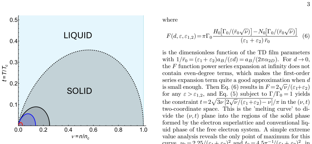
By reducing material thickness the authors show that the critical electron density for Wigner crystallization falls low enough to reach room temperature. Electrons then pin to a two-dimensional triangular lattice of a supersolid inside the crystalline material. The solid melts and freezes reversibly with increasing or decreasing electron doping or temperature, and its resistivity behaves opposite to free-electron-gas predictions.
What carries the argument
Thickness-tuned effective Coulomb interactions that set the critical density and melting curve for Wigner crystallization in transdimensional materials.
If this is right
- Electrons form a supersolid pinned to a two-dimensional triangular lattice inside the host crystal.
- The solid melts and refreezes reversibly when electron doping or temperature is changed.
- Resistivity increases with added electron density, opposite to free-electron-gas behavior.
- Crystallization occurs at room temperature once thickness is reduced sufficiently.
Where Pith is reading between the lines
- Thickness control could be used to create temperature- or doping-tunable switches between ordered and conducting states in thin films.
- The same dimensional tuning might apply to other interaction-driven phases in low-dimensional electron systems.
- Direct tests would require transport measurements on fabricated ultrathin samples while varying thickness and carrier density.
Load-bearing premise
The model that links material thickness directly to the strength of electron interactions is accurate enough to produce room-temperature crystallization without higher-order corrections or extra constraints.
What would settle it
An experiment on a predicted ultrathin material that finds the crystallization temperature remains below room temperature even at the smallest achievable thicknesses would disprove the central claim.
Figures


read the original abstract
Wigner crystallization of free electrons at room temperature is explored for a new class of metallic ultrathin (transdimensional) materials whose properties can be controlled by their thickness. Our calculations of the critical electron density, temperature and the melting curve show that by reducing the material thickness one can Wigner-crystallize free electrons at room temperature to get them pinned onto a two-dimensional triangular lattice of a supersolid inside of the crystalline material. Such a solid melts and freezes reversibly with increase and decrease of electron doping or temperature, whereby its resistivity behaves opposite to the free electron gas model predictions.
Editorial analysis
A structured set of objections, weighed in public.
Referee Report
Summary. The manuscript explores Wigner crystallization of free electrons in ultrathin transdimensional metallic materials, claiming that reducing thickness enhances effective interactions to enable room-temperature crystallization. Electrons are predicted to pin onto a two-dimensional triangular lattice forming a supersolid inside the host crystal. Calculations of critical electron density, temperature, and the melting curve are presented, with the solid melting and freezing reversibly upon changes in doping or temperature and resistivity behaving opposite to free-electron-gas predictions.
Significance. If the thickness-dependent interaction model and resulting critical curves hold after validation, the result would be significant for the field of strongly correlated electrons in low-dimensional systems. It would demonstrate a route to ambient-condition Wigner crystals and supersolids whose phase can be tuned by thickness, doping, or temperature, potentially enabling new studies of pinned electron lattices and anomalous transport in controllable materials.
major comments (2)
- [Model and results sections (equations for transdimensional potential and critical curves)] The thickness-dependent Coulomb interaction model (central to all calculations of critical density, temperature, and melting curve) is not validated against the established 3D Wigner threshold (r_s ≳ 100) or 2D threshold (r_s ≳ 30–40). Without these limits or explicit checks on the functional form, the extrapolation to room-temperature crystallization cannot be assessed for correctness.
- [Calculations of melting curve and critical parameters] No higher-order corrections for material screening, lattice pinning, or quantum fluctuations are included or estimated, yet these directly affect whether the electrons remain free enough to form the claimed 2D triangular lattice at the reported densities and temperatures.
minor comments (2)
- [Abstract] The abstract refers to 'calculations' without naming the approximations, numerical methods, or software used; this should be stated explicitly even if details appear later.
- [Throughout] Notation for the effective r_s or equivalent interaction parameter should be defined once and used consistently when comparing to 2D/3D literature values.
Simulated Author's Rebuttal
We thank the referee for their careful reading of the manuscript and for highlighting these important points regarding validation and corrections. We respond to each major comment below.
read point-by-point responses
-
Referee: [Model and results sections (equations for transdimensional potential and critical curves)] The thickness-dependent Coulomb interaction model (central to all calculations of critical density, temperature, and melting curve) is not validated against the established 3D Wigner threshold (r_s ≳ 100) or 2D threshold (r_s ≳ 30–40). Without these limits or explicit checks on the functional form, the extrapolation to room-temperature crystallization cannot be assessed for correctness.
Authors: We agree that explicit checks against the established 3D (r_s ≳ 100) and 2D (r_s ≳ 30–40) Wigner thresholds are necessary to validate the functional form of the thickness-dependent interaction and to support the extrapolation. The model is constructed to recover the 3D Coulomb form at large thickness and the 2D form at small thickness. In the revised manuscript we will add explicit calculations demonstrating recovery of the literature thresholds in the appropriate limits. revision: yes
-
Referee: [Calculations of melting curve and critical parameters] No higher-order corrections for material screening, lattice pinning, or quantum fluctuations are included or estimated, yet these directly affect whether the electrons remain free enough to form the claimed 2D triangular lattice at the reported densities and temperatures.
Authors: The calculations focus on the leading thickness dependence of the interaction. We acknowledge that screening, pinning, and quantum fluctuations are relevant and were not estimated in the original submission. In revision we will add order-of-magnitude estimates of these effects to assess their influence on the reported critical densities and temperatures. revision: yes
Circularity Check
No circularity; derivation chain not reducible to inputs in provided text
full rationale
The abstract and skeptic summary describe a model for thickness-dependent Coulomb interactions and resulting critical density/temperature curves for Wigner crystallization, but no equations, fitting procedures, or self-citations are quoted that would allow reduction of any prediction to a fitted parameter or self-referential definition. The central claim rests on an assumed functional form whose accuracy is questioned externally, yet this is a correctness issue rather than a circularity issue per the rules. No self-definitional steps, fitted inputs renamed as predictions, or load-bearing self-citations are exhibited. The derivation is treated as self-contained against external benchmarks until specific reductions can be shown from the full manuscript.
Axiom & Free-Parameter Ledger
Lean theorems connected to this paper
-
IndisputableMonolith/Cost/FunctionalEquation.leanwashburn_uniqueness_aczel unclear?
unclearRelation between the paper passage and the cited Recognition theorem.
VKR(ρ) = e²π/(ε1+ε2)r0 [H0(ρ/r0)−N0(ρ/r0)] … Γ = ⟨VKR⟩/⟨K⟩ … melting surface Eq. (7)
-
IndisputableMonolith/Foundation/RealityFromDistinction.leanreality_from_one_distinction unclear?
unclearRelation between the paper passage and the cited Recognition theorem.
transdimensional (TD) material platform … thickness d … Wigner crystal phase
What do these tags mean?
- matches
- The paper's claim is directly supported by a theorem in the formal canon.
- supports
- The theorem supports part of the paper's argument, but the paper may add assumptions or extra steps.
- extends
- The paper goes beyond the formal theorem; the theorem is a base layer rather than the whole result.
- uses
- The paper appears to rely on the theorem as machinery.
- contradicts
- The paper's claim conflicts with a theorem or certificate in the canon.
- unclear
- Pith found a possible connection, but the passage is too broad, indirect, or ambiguous to say the theorem truly supports the claim.
Reference graph
Works this paper leans on
-
[1]
E.Wigner, On the Interaction of Electrons in Metals, Phys. Rev. 46, 1002 (1934)
work page 1934
-
[2]
P.W.Anderson, Absence of diffusion in certain random lattices, Phys. Rev. 109, 1492 (1958)
work page 1958
-
[3]
J.Kondo, Resistance minimum in dilute magnetic alloys, Progr. Theor. Phys. 32, 37 (1964)
work page 1964
-
[4]
W.H.Kleiner, L.M.Roth, and S.H.Autler, Bulk solution of Ginzburg-Landau equations for type II superconduc- tors: Upper critical field region, Phys. Rev. 133, A1226 (1964)
work page 1964
-
[5]
R.Williams, R.Crandall, and A.Willis, Surface states of electrons on liquid helium, Phys. Rev. Lett. 26, 7 (1971)
work page 1971
-
[6]
J.M.Kosterlitz and D.J.Thouless, Ordering, metastabil- ity and phase transitions in two-dimensional systems, J. Phys. C: Solid State Phys. 6, 11 81 (1973)
work page 1973
-
[7]
P.M.Platzman and H.Fukuyama, Phase diagram of the two-dimensional electron liquid, Phys. Rev. B 10, 3150 (1974)
work page 1974
-
[8]
Yu.E.Lozovik and V.I.Yudson, A new mechanism for superconductivity: pairing between spatially separated electrons and holes, Sov. Phys. JETP 44, 389 (1976)
work page 1976
-
[9]
C.C.Grimes C.C. and G.Adams, Evidence for a liquid-to- crystal phase transition in a classical, two-Dimensional sheet of electrons, Phys. Rev. Lett. 42, 795 (1979)
work page 1979
-
[10]
H.Fukuyama, P.M.Platzman, and P.W.Anderson, Two- Dimensional electron gas in a strong magnetic field, Phys. Rev. B 19, 5211 (1979)
work page 1979
-
[11]
Lozovik, V.M.Farztdinov, and B.Abdullaev, 2D electron crystal in quantized magnetic field: Melting induced by zero-point oscillations, J. Phys. C: Solid State Phys. 18, L807 (1985)
work page 1985
-
[12]
V.Goldman, M.Santos, M.Shayegan, and J.Cunningham, Evidence for two-dimensional quantum Wigner crystal, Phys. Rev. Lett. 65, 2189 (1990)
work page 1990
-
[13]
M.M.Fogler, L.V.Butov, and K.S.Novoselov, High- T su- perfluidity with indirect excitons in van der Waals het- erostructures, Nature Commun. 5, 4555 (2014)
work page 2014
-
[14]
R.A.Suris, Gas-crystal phase transition in a 2D dipolar exciton system, JETP 122, 602 (2016)
work page 2016
-
[15]
Y.E.Lozovik, New effects in and the control of the exci- ton system in quasi-two-dimensional structures, Physics– Uspekhi 61, 1094 (2018)
work page 2018
-
[16]
Z.Sun, J.Beaumariage, Q.Wan, H.Alnatah, N.Hougland, J.Chisholm, Q.Cao, K.Watanabe, T.Taniguchi, B.M. Hunt, I.V.Bondarev, and D.Snoke, Charged bosons made of fermions in bilayer structures with strong metallic screening, Nano Lett. 21, 7669 (2021)
work page 2021
-
[17]
Snoke, Light-induced electron pairing in a bilayer structure, arXiv:2412.06941 (12 Dec 2024)
Q.Wan, D.Vaz, L.Xiang, A.Ramavath, B.Vargo, J.Ye, J.Beaumariage, K.Watanabe, T.Taniguchi, Z.Sun, D.Smirnov, N.Youngblood, I.V.Bondarev, and D.W. Snoke, Light-induced electron pairing in a bilayer structure, arXiv:2412.06941 (12 Dec 2024)
-
[18]
A.Dikopoltsev, S.Weidemann, M.Kremer, A.Steinfurth, H.H.Sheinfux, A.Szameit, and M.Segev, Observation of Anderson localization beyond the spectrum of the disor- der, Science Adv. 8, eabn7769 (2022)
work page 2022
-
[19]
A.Demuth, R.Camphausen, A.Cuevas, N.F.Borrelli, T.P.Seward III, L.Lamberson, K.W.Koch, A.Ruggeri, F.Madonini, F.Villa, and V.Pruneri, Quantum light transport in phase-separated Anderson localization fiber, Commun. Phys. 5, 261 (2022)
work page 2022
-
[20]
H.Zhou, H.Polshyn, T.Taniguchi, K.Watanabe, and A.F.Young, Solids of quantum Hall skyrmions in graphene, Nature Phys. 16, 154 (2020)
work page 2020
-
[21]
S.M.Cronenwett, T.H.Oosterkamp, and L.P.Kouwen- hoven, A tunable Kondo effect in quantum dots, Science 281, 540 (1998)
work page 1998
-
[22]
K.Noro, Y.Kozuka, K.Matsumura, T.Kumasaka, Y.Fuji- wara, A.Tsukazaki, M.Kawasaki, and T.Otsuka, Parity- independent Kondo effect of correlated electrons in elec- trostatically defined ZnO quantum dots, Nature Com- mun. 15, 9556 (2024)
work page 2024
-
[23]
V.V.Deshpande and M.Bockrath, The one-dimensional Wigner crystal in carbon nanotubes, Nature Phys. 4, 314 (2008)
work page 2008
-
[24]
I.Shapir, A.Hamo, S.Pecker, C.P.Moca, ¨O.Legeza, G.Zarand, and S.Ilani, Imaging the electronic Wigner crystal in one dimension, Science 364, 870 (2019)
work page 2019
-
[25]
Ashoori, Sharp tunnelling resonance from the vibrations of an electronic Wigner crystal, Nature Phys
J.Jang, B.M.Hunt, L.N.Pfeiffer, K.W.West, and R.C. Ashoori, Sharp tunnelling resonance from the vibrations of an electronic Wigner crystal, Nature Phys. 13, 340 (2017)
work page 2017
-
[26]
Y.-C.Tsui, M.He, Y.Hu, E.Lake, T.Wang, K.Watanabe, T.Taniguchi, M.P.Zaletel, and A.Yazdani, Direct obser- vation of a magnetic-field induced Wigner crystal, Nature 628, 287 (2024)
work page 2024
-
[27]
T.Smole´ nski, P.E.Dolgirev, C.Kuhlenkamp, A.Popert, Y.Shimazaki, P.Back, X.Lu, M.Kroner, K.Watanabe, T.Taniguchi, I.Esterlis, E.Demler, and A.Imamo˘ glu, Sig- natures of Wigner crystal of electrons in a monolayer semiconductor, Nature 595, 53 (2021)
work page 2021
-
[28]
Y.Zhou, J.Sung, E.Brutschea, I.Esterlis, Y.Wang, 6 G.Scuri, R.J.Gelly, H.Heo, T.Taniguchi, K.Watanabe, G.Zar´ and, M.D.Lukin, P.Kim, E.Demler, and H.Park, Bilayer Wigner crystals in a transition metal dichalco- genide heterostructure, Nature 595, 48 (2021)
work page 2021
-
[29]
E.C.Regan, D.Wang, C.Jin, I.B.Utama, B.Gao, X.Wei, S.Zhao, W.Zhao, Z.Zhang, K.Yumigeta, M.Blei, J.D.Carlstr¨ om, K.Watanabe, T.Taniguchi, S.Tongay, M.Crommie, A.Zettl, and F.Wang, Mott and generalized Wigner crystal states in WSe 2/WS2 moir´ e superlattices, Nature 579, 359 (2020)
work page 2020
-
[30]
H.Li, S.Li, E.C.Regan, D.Wang, W.Zhao, S.Kahn, K.Yu- migeta, M.Blei, T.Taniguchi, K.Watanabe, S.Tongay, A.Zettl, M.F.Crommie, and F.Wang, Imaging two- dimensional generalized Wigner crystals, Nature 597, 650 (2021)
work page 2021
-
[31]
H.Li, Z.Xiang, A.P.Reddy, T.Devakul, R.Sailus, R.Ba- nerjee, T.Taniguchi, K.Watanabe, S.Tongay, A.Zettl, L.Fu, M.F.Crommie, and F.Wang, Wigner molecular crystals from multielectron moir¨ e artificial atoms, Sci- ence 385, 86 (2024)
work page 2024
-
[32]
Crommie, and F.Wang, Mapping charge excitations in generalized Wigner Crystals, Nature Nanotechnol
H.Li, Z.Xiang, E.C.Regan, W.Zhao, R.Sailus, R.Baner- jee, T.Taniguchi, K.Watanabe, S.Tongay, A.Zettl, M.F. Crommie, and F.Wang, Mapping charge excitations in generalized Wigner Crystals, Nature Nanotechnol. 19, 618 (2024)
work page 2024
-
[33]
Y.Xu, S.Liu, D.A.Rhodes, K.Watanabe, T.Taniguchi, J.Hone, V.Elser, K.F.Mak, and J.Shan, Correlated insu- lating states at fractional fillings of moir´ e superlattices, Nature 587, 214 (2020)
work page 2020
-
[34]
Watanabe, T.Taniguchi, J.Hone, L.Fu, J.Shan, and K.F
C.Jin, Z.Tao, T.Li, Y.Xu, Y.Tang, J.Zhu, S.Liu, K. Watanabe, T.Taniguchi, J.Hone, L.Fu, J.Shan, and K.F. Mak, Stripe phases in WSe 2/WS2 moir´ e superlattices, Nature Mater. 20, 940 (2021)
work page 2021
-
[35]
X.Huang, T.Wang, S.Miao, C.Wang, Z.Li, Z.Lian, T.Taniguchi, K.Watanabe, S.Okamoto, D.Xiao, S.-F.Shi, and Y.-T.Cui, Correlated insulating states at fractional fillings of the WS2/WSe2 moir´ e lattice, Nature Phys. 17, 715 (2021)
work page 2021
-
[36]
H.D.Scammell, J.Ingham, T.Li, and O.P.Sushkov, Chiral excitonic order from twofold van Hove singularities in kagome metals, Nature Commun. 14, 605 (2023)
work page 2023
-
[37]
L.Ma, P.X.Nguyen, Z.Wang, Y.Zeng, K.Watanabe, T.Taniguchi, A.H.MacDonald, K.F.Mak, and J.Shan, Strongly correlated excitonic insulator in atomic double layers, Nature 598, 585 (2021)
work page 2021
-
[38]
Y.N.Joglekar, A.V.Balatsky, and S.Das Sarma, Wigner supersolid of excitons in electron-hole bilayers, Phys. Rev. B 74, 233302 (2006)
work page 2006
-
[39]
Lozovik, Crystal phases of charged interlayer excitons in van der Waals heterostructures, Commun
I.V.Bondarev, O.L.Berman, R.Y.Kezerashvili, and Y.E. Lozovik, Crystal phases of charged interlayer excitons in van der Waals heterostructures, Commun. Phys. 4, 134 (2021)
work page 2021
-
[40]
I.V.Bondarev and Y.E.Lozovik, Magnetic-field-induced Wigner crystallization of charged interlayer excitons in van der Waals heterostructures, Commun. Phys. 5, 315 (2022)
work page 2022
-
[41]
X.Sun, Y.Zhu, H.Qin, B.Liu, Y.Tang, T.L¨ u, S.Rahman, T.Yildirim, and Y.Lu, Enhanced interactions of inter- layer excitons in free-standing heterobilayers, Nature 610, 478 (2022)
work page 2022
-
[42]
D.D.Dai and L.Fu, Strong-coupling phases of trions and excitons in electron-hole bilayers at commensurate den- sities, Phys. Rev. Lett. 132, 196202 (2024)
work page 2024
-
[43]
Y.P.Monarkha and V.E.Syvokon, A two-dimensional Wi- gner crystal (Review Article), Low Temp. Phys. 38, 1067 (2012)
work page 2012
-
[44]
D.Shah, Z.A.Kudyshev, S.Saha, V.M.Shalaev, and A.Bo- ltasseva, Transdimensional material platforms for tun- able metasurface design, MRS Bulletin 45, 188 (2020)
work page 2020
-
[45]
A.Boltasseva and V.M.Shalaev, Transdimensional pho- tonics, ACS Photonics 6, 1 (2019)
work page 2019
-
[46]
R.A.Maniyara, D.Rodrigo, R.Yu, J.Canet-Ferrer, D.S.Ghosh, R.Yongsunthon, D.E.Baker, A.Rezikyan, F.J.Garc´ ıa de Abajo, and V.Pruneri, Tunable plasmons in ultrathin metal films, Nature Photonics 13, 328 (2019)
work page 2019
-
[47]
A.Manjavacas and F.J.Garc´ ıa de Abajo, Tunable plas- mons in atomically thin gold nanodisks, Nature Com- mun. 5, 3548 (2014)
work page 2014
-
[48]
S.A.Maier and H.A.Atwater, Plasmonics: Localization and guiding of electromagnetic energy in metal/dielectric structures. J. Appl. Phys. 98, 011101 (2005)
work page 2005
-
[49]
A.Boltasseva, I.V.Bondarev, and V.M.Shalaev, Transdi- mensional materials as a new platform for strongly cor- related systems, in: Roadmap on Atomically Thin Pho- tonic Materials, ACS Photonics 2025, in print
work page 2025
-
[50]
I.V.Bondarev and V.M.Shalaev, Universal features of the optical properties of ultrathin plasmonic films, Opt. Mater. Express 7, 3731 (2017)
work page 2017
-
[51]
I.V.Bondarev, H.Mousavi, and V.M.Shalaev, Optical re- sponse of finite-thickness ultrathin plasmonic films, MRS Commun. 8, 1092 (2018)
work page 2018
-
[52]
I.V.Bondarev, H.Mousavi, and V.M.Shalaev, Transdi- mensional epsilon-near-zero modes in planar plasmonic nanostructures, Phys. Rev. Research 2, 013070 (2020)
work page 2020
-
[53]
I.V.Bondarev, Controlling single-photon emission with ultrathin transdimensional plasmonic films, Ann. Phys. (Berlin) 535, 2200331 (2023)
work page 2023
-
[54]
S.-A.Biehs and I.V.Bondarev, Goos-H¨ anchen effect singularities in transdimensional plasmonic films, arXiv:2410.09308v2 (18 Dec 2024)
work page internal anchor Pith review Pith/arXiv arXiv 2024
-
[55]
G.V.Naik, V.M.Shalaev, and A.Boltasseva, Alternative plasmonic materials: Beyond gold and silver. Adv. Mater. 25, 3264 (2013)
work page 2013
-
[56]
S.-A.Biehs and I.V.Bondarev, Far- and Near-Field Heat Transfer in Transdimensional Plasmonic Film Systems, Adv. Optical Mater. 11, 2202712 (2023)
work page 2023
-
[57]
D.Shah, M.Yang, Z.Kudyshev, X.Xu, V.M.Shalaev, I.V.Bondarev, and A.Boltasseva, Thickness-dependent Drude plasma frequency in transdimensional plasmonic TiN, Nano Lett. 22, 4622 (2022)
work page 2022
-
[58]
P.Das, S.Rudra, D.Rao, S.Banerjee, A.I.Kamalasanan Pillai, M.Garbrecht, A.Boltasseva, I.V.Bondarev, V.M. Shalaev, and B.Saha, Electron confinement-induced plas- monic breakdown in metals, Science Advances 10, eadr2596 (2024)
work page 2024
-
[59]
H.Salihoglu, J.Shi, Z.Li, Z.Wang, X.Luo, I.V.Bondarev, S.-A.Biehs, and S.Shen, Nonlocal near-field radiative heat transfer by transdimensional plasmonics, Phys. Rev. Lett. 131, 086901 (2023)
work page 2023
-
[61]
P.Cudazzo, I.V.Tokatly, and A.Rubio, Dielectric screen- ing in two-dimensional insulators: Implications for exci- tonic and impurity states in graphane, Phys. Rev. B 84, 7 085406 (2011)
work page 2011
-
[62]
I.V.Bondarev, A.Boltasseva, and V.M.Shalaev, Supple- mentary information file for this article
-
[63]
A.A.Balandin and D.L.Nika, Phononics in low-dimensi- onal materials, Mater. Today 15, 266 (2012)
work page 2012
-
[64]
A.Laturia, M.L.Van de Put, and W.G.Vandenberghe, Di- electric properties of hexagonal boron nitride and transi- tion metal dichalcogenides: from monolayer to bulk, npj 2D Mater. & Appl. 2, 6 (2018)
work page 2018
-
[65]
J.Yoon, C.C.Li, D.Shahar, D.C.Tsui, and M.Shayegan, Wigner crystallization and metal-insulator transition of two-dimensional holes in GaAs at B =0, Phys. Rev. Lett. 82, 1744 (1999)
work page 1999
-
[66]
B.Tanatar and D.M.Ceperley, Ground state of the two- dimensional electron gas, Phys. Rev. B 39, 5050 (1989)
work page 1989
-
[67]
K.Hirabayashi, Dielectric theory of the barrier height at metal-semiconductor and metal-insulator interfaces, Phys. Rev. B 3, 4023 (1971)
work page 1971
-
[68]
Y.Qi, A.Sadi, D.Hu, M.Zheng, Z.Wu, Y.Jiang, and Y.P.Chen, Recent progress in strain engineering on Van der Waals 2D materials: Tunable electrical, electrochem- ical, magnetic, and optical Properties, Adv. Mater. 35, 2205714 (2023). Supplementary Information Crystallization of the Transdimensional Electron Liquid Igor V. Bondarev, 1 Alexandra Boltasseva,2,...
work page internal anchor Pith review Pith/arXiv arXiv 2023
-
[69]
P.Cudazzo, I.V.Tokatly, and A.Rubio, Dielectric screening in two-dimensional insulators: Implications for excitonic and impurity states in graphane, Phys. Rev. B 84, 085406 (2011)
work page 2011
-
[70]
J.Deslippe, M.Dipoppa, D.Prendergast, M.V.O.Moutinho, R.B.Capaz, and S.G.Louie, Electron-hole interaction in carbon nanotubes: novel screening and exciton excitation spectra, Nano Lett. 9, 1330 (2009)
work page 2009
-
[71]
L.V.Keldysh, Coulomb interaction in thin semiconductor and semimetal films, Pis’ma Zh. Eksp. Teor. Fiz. 29, 716 (1979) [Engl. translation: JETP Lett. 29, 658 (1979)]; N.S.Rytova, Screened potential of a point charge in a thin film, Moscow University Physics Bulletin 3, 30 (1967)
work page 1979
-
[72]
L.D.Landau and E.M.Lifshitz, Statistical Physics, Part 1 (Course of Theoretical Physics, V.5), 3rd ed., Oxford, 1980
work page 1980
-
[73]
B.Tanatar and D.M.Ceperley, Ground state of the two-dimensional electron gas, Phys. Rev. B 39, 5050 (1989)
work page 1989
-
[74]
T.Smole´ nski, P.E.Dolgirev, C.Kuhlenkamp, A.Popert, et al., Signatures of Wigner crystal of electrons in a monolayer semiconductor, Nature 595, 53 (2021); Y.Zhou, J.Sung, E.Brutschea, I.Esterlis, et al., Bilayer Wigner crystals in a transition metal dichalcogenide heterostructure, ibid. 595, 48 (2021)
work page 2021
-
[75]
J.Yoon, C.C.Li, D.Shahar, D.C.Tsui, and M.Shayegan, Wigner crystallization and metal-insulator transition of two- dimensional holes in GaAs at B =0, Phys. Rev. Lett. 82, 1744 (1999). 6 FIG. S1. The domain of the PF model melting curve (23) is the light-red shaded area bounded by the functions √νandνfrom the top and bottom, respectively. FIG. S2. The domai...
work page 1999
discussion (0)
Sign in with ORCID, Apple, or X to comment. Anyone can read and Pith papers without signing in.