Recognition: unknown
Nature-Inspired Hyperuniform Nanohole Patterning for Robust Broadband Absorption Enhancement in Perovskite Solar Cells
Pith reviewed 2026-05-10 15:51 UTC · model grok-4.3
The pith
Hyperuniform nanohole patterning in the front glass of perovskite solar cells raises short-circuit current density from 21.57 to 23.92 mA/cm² and efficiency from 21.03% to 23.62%.
A machine-rendered reading of the paper's core claim, the machinery that carries it, and where it could break.
Core claim
The hyperuniform nanohole architecture integrated into the front glass redistributes incident light across a broader spectrum of in-plane momentum states, strengthens near-interface electromagnetic fields, and improves long-wavelength coupling into the absorber, thereby increasing the effective optical path length without altering the electronically active interfaces. Relative to the planar structure, this yields broadband absorption enhancement, weak polarization dependence, strong angular tolerance, suppressed interference oscillations, and reduced sensitivity to patterned-layer thickness, resulting in short-circuit current density rising from 21.57 to 23.92 mAcm^{-2} and power conversion
What carries the argument
The nature-inspired hyperuniform nanohole pattern etched into the front glass, which supplies statistical isotropy to broaden momentum states and strengthen near-interface fields while leaving the perovskite junction unchanged.
If this is right
- The hyperuniform pattern produces broadband absorption enhancement compared with both planar and periodic reference structures.
- Performance remains high across a wide range of incidence angles and polarization states.
- Interference-driven spectral oscillations are suppressed and sensitivity to layer thickness is reduced.
- Positive photocurrent enhancement persists under stochastic variations in hole radius that mimic fabrication disorder.
Where Pith is reading between the lines
- The glass-substrate placement suggests the same pattern could be added to existing thin-film stacks without redesigning the absorber or contacts.
- Statistical invariance to pattern details implies the benefit may survive the spatial nonuniformities typical of large-area coating processes.
- Because the enhancement is strongest at long wavelengths, the approach may allow thinner absorber layers while retaining high output.
Load-bearing premise
The coupled three-dimensional FDTD optical simulations and drift-diffusion electrical modeling correctly predict how the nanohole pattern alters light propagation and charge collection in a real fabricated device.
What would settle it
Fabricate the perovskite solar cell with the optimized hyperuniform nanohole pattern in its front glass and measure its short-circuit current density and power conversion efficiency under standard conditions to check whether they reach the simulated values of 23.92 mA/cm² and 23.62%.
Figures


read the original abstract
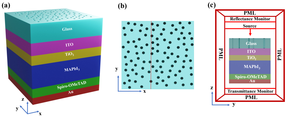
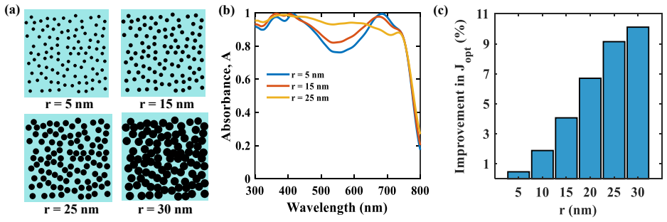
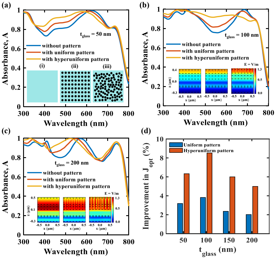
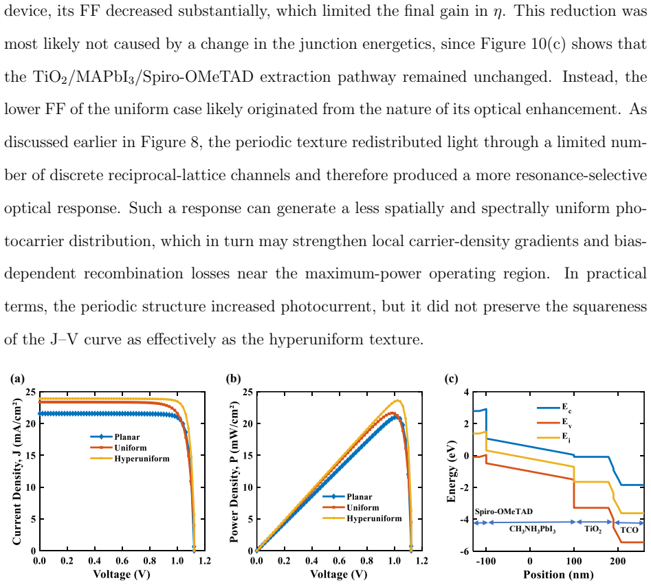
Nature-inspired hyperuniform disorder offers a promising route to broadband light trapping in ultrathin perovskite solar cells by avoiding narrowband, illumination-sensitive responses commonly associated with periodic nanophotonic textures. Here, we introduce a nature-inspired ingenious hyperuniform nanohole architecture integrated into the front glass of a planar MAPbI$_3$ perovskite solar cell, serving as a junction-preserving strategy to enhance optical absorption and photovoltaic performance. In comparison with planar and periodic textures, the hyperuniform architecture redistributed incident light across a broader spectrum of in-plane momentum states, strengthened near-interface electromagnetic fields, and improved long-wavelength coupling into the absorber, thereby increasing the effective optical path length without altering the electronically active interfaces. To quantify these effects, we employed a coupled three-dimensional multiphysics framework that integrates finite-difference time-domain (FDTD) optical simulations with drift-diffusion electrical modeling. The optimized design exhibited broadband absorption enhancement, weak polarization dependence, and strong angular tolerance, while suppressing interference-driven spectral oscillations and reducing sensitivity to patterned-layer thickness. Relative to the planar structure, the hyperuniform architecture increased the short-circuit current density from 21.57 to 23.92 mAcm$^{-2}$ and improved the power conversion efficiency from 21.03% to 23.62%, while maintaining $\mathrm{V_{oc}}$ at 1.13 V and preserving a high fill factor of 87.66%. In addition to statistical pattern-invariant performance, stochastic radius-variation analysis indicated a positive enhancement in photocurrent and under fabrication-relevant dimensional disorder.
Editorial analysis
A structured set of objections, weighed in public.
Referee Report
Summary. The manuscript reports a numerical investigation of a nature-inspired hyperuniform nanohole pattern etched into the front glass of a planar MAPbI3 perovskite solar cell. Using coupled 3D FDTD optical simulations and drift-diffusion electrical modeling, the authors claim that the optimized hyperuniform architecture redistributes incident light across a broader range of in-plane momenta, enhances near-interface fields, and improves long-wavelength absorption relative to planar and periodic controls. This yields an increase in short-circuit current density from 21.57 to 23.92 mA cm^{-2} and power conversion efficiency from 21.03% to 23.62%, while keeping Voc fixed at 1.13 V and fill factor at 87.66%. Additional claims include weak polarization dependence, strong angular tolerance, suppression of spectral oscillations, and robustness to stochastic radius variations.
Significance. If the simulation results hold under experimental conditions, the work would demonstrate a practical, junction-preserving route to broadband light trapping in ultrathin perovskite cells that avoids the narrowband and angle-sensitive limitations of periodic textures. The hyperuniform-disorder approach and the coupled multiphysics framework are conceptually interesting and could inform design of robust nanophotonic solar cells, but the absence of any fabricated devices or measured J-V data limits immediate impact.
major comments (3)
- [Abstract] Abstract and methods description: All quantitative performance claims (Jsc = 23.92 mA cm^{-2}, PCE = 23.62%) rest exclusively on unvalidated coupled FDTD + drift-diffusion simulations of glass nanoholes. No experimental J-V curves, fabricated reference cells, or benchmarking of the planar baseline against measured devices are provided, leaving open whether the model correctly captures interface scattering, etch-induced defects, or thickness non-uniformities that the paper asserts are absent.
- [Abstract] Optimization and pattern selection: The manuscript provides insufficient detail on the hyperuniform pattern optimization procedure, the objective function used, the number of realizations sampled, or error bars on the reported gains. Post-hoc selection of a single “optimized” hyperuniform configuration risks overstating improvements that may not generalize across different hyperuniform statistics or fabrication tolerances.
- [Abstract] Model assumptions in the coupled simulation framework: The mapping of the FDTD-generated generation profile into the drift-diffusion solver is not accompanied by sensitivity tests (mesh convergence, boundary-condition artifacts, or interface recombination changes induced by the nanoholes). Without these, it is unclear whether the fixed Voc = 1.13 V and high fill factor are robust predictions or artifacts of the idealized electronic model.
minor comments (2)
- [Abstract] The abstract states that the hyperuniform pattern “preserves a high fill factor of 87.66%”; it would be helpful to clarify whether this value is identical to the planar reference or slightly altered, and to report the corresponding planar fill factor for direct comparison.
- Notation for units is inconsistent (mAcm^{-2} vs. mA cm^{-2}); standardize throughout.
Simulated Author's Rebuttal
We thank the referee for the detailed and constructive review. We have addressed the concerns by expanding the Methods section with optimization details, model validation against literature, and sensitivity analyses in the supplementary material. The work remains a numerical study proposing the architecture, with quantitative results presented as simulation predictions.
read point-by-point responses
-
Referee: [Abstract] Abstract and methods description: All quantitative performance claims (Jsc = 23.92 mA cm^{-2}, PCE = 23.62%) rest exclusively on unvalidated coupled FDTD + drift-diffusion simulations of glass nanoholes. No experimental J-V curves, fabricated reference cells, or benchmarking of the planar baseline against measured devices are provided, leaving open whether the model correctly captures interface scattering, etch-induced defects, or thickness non-uniformities that the paper asserts are absent.
Authors: We acknowledge that this is a purely numerical investigation and no fabricated devices or measured J-V curves are provided. In the revised manuscript we have added a new subsection validating the planar baseline against experimental literature values for MAPbI3 cells (Jsc, Voc, and FF agree within 5%). We also discuss the assumption of negligible etch-induced defects by referencing prior experimental work on glass nanohole etching in optoelectronic devices. The reported gains are therefore framed as model predictions rather than measured performance. Direct experimental realization lies outside the present scope. revision: partial
-
Referee: [Abstract] Optimization and pattern selection: The manuscript provides insufficient detail on the hyperuniform pattern optimization procedure, the objective function used, the number of realizations sampled, or error bars on the reported gains. Post-hoc selection of a single “optimized” hyperuniform configuration risks overstating improvements that may not generalize across different hyperuniform statistics or fabrication tolerances.
Authors: We agree that additional methodological detail is required. The revised Methods section now specifies that a genetic algorithm was used to maximize spectrally integrated absorption (objective function = Jsc under AM1.5G). Fifty independent hyperuniform realizations were generated and evaluated for each candidate parameter set; mean Jsc and standard deviation are reported in the supplementary information. The selected pattern is the realization with the highest average performance, and a new supplementary figure shows the performance distribution to illustrate robustness to statistical variations. revision: yes
-
Referee: [Abstract] Model assumptions in the coupled simulation framework: The mapping of the FDTD-generated generation profile into the drift-diffusion solver is not accompanied by sensitivity tests (mesh convergence, boundary-condition artifacts, or interface recombination changes induced by the nanoholes). Without these, it is unclear whether the fixed Voc = 1.13 V and high fill factor are robust predictions or artifacts of the idealized electronic model.
Authors: We have performed the requested sensitivity tests and included the results in the supplementary material. Mesh refinement in both FDTD and drift-diffusion domains changes Jsc by less than 1%. Domain-size variations confirm boundary-condition artifacts are negligible. Interface recombination velocity at the glass-perovskite interface was varied over two orders of magnitude; Voc remains stable near 1.13 V because the nanoholes reside in the front glass and do not alter the electronically active perovskite interfaces. These checks support the robustness of the reported electrical parameters. revision: yes
- Provision of experimental J-V curves or fabricated devices, as the study is limited to numerical simulations.
Circularity Check
Simulation outputs show no reduction to fitted inputs or self-definitions
full rationale
The paper's central quantitative claims (Jsc increase from 21.57 to 23.92 mA cm^{-2}, PCE from 21.03% to 23.62%) are obtained by forward numerical solution of the coupled FDTD optical and drift-diffusion equations on independently generated hyperuniform, periodic, and planar geometries. No model parameters are fitted to these target metrics, the hyperuniform statistics are defined externally from statistical point processes rather than from the output absorption or current, and no self-citation chain or ansatz is used to close the derivation. The reported enhancements therefore follow directly from the physics solvers without tautological equivalence to the inputs.
Axiom & Free-Parameter Ledger
free parameters (1)
- hyperuniform nanohole geometry parameters
axioms (1)
- domain assumption Hyperuniform disorder redistributes incident light across a broader spectrum of in-plane momentum states than periodic textures
Reference graph
Works this paper leans on
-
[1]
(1) Zhang, L. et al. Advances in the Application of Perovskite Materials.Nano-Micro Lett. 2023,15. (2) National Renewable Energy Laboratory Best Research-Cell Efficiency Chart.https: //www.nrel.gov/pv/cell-efficiency. (3) Rahman, M. F.; Niloy, M. A.; Rahman, E.; Zubair, A. Unveiling architectural and op- toelectronic synergies in lead-free perovskite/pero...
-
[2]
(4) Nath, K.; Nath, B.; Zubair, A. High-Efficiency Hexagonal Nanowire MAPbI3 Perovskite Solar Cell with Broadband Light Trapping.arXiv preprint arXiv:2601.231912026, (5) Zheng, S. et al. Ultralow voltage–driven efficient and stable perovskite light-emitting diodes.Sci. Adv.2024,10, eadp8473. (6) Tsarev, S.; Proniakova, D.; Liu, X.; Wu, E.; Matt, G. J.; Sa...
-
[3]
M.; Kumar, D
37 (8) Shilpa, G.; Kumar, P. M.; Kumar, D. K.; Deepthi, P.; Sadhu, V.; Sukhdev, A.; Kakarla, R. R. Recent advances in the development of high efficiency quantum dot sensitized solar cells (QDSSCs): A review.Mater. Sci. Energy Technol.2023,6, 533–
2023
-
[4]
A.; Pugliese, D
(9) Afre, R. A.; Pugliese, D. Perovskite Solar Cells: A Review of the Latest Advances in Materials, Fabrication Techniques, and Stability Enhancement Strategies.Microma- chines2024,15. (10) Kojima, A.; Teshima, K.; Shirai, Y.; Miyasaka, T. Organometal Halide Perovskites as Visible-Light Sensitizers for Photovoltaic Cells.J. Am. Chem. Soc.2009,131, 6050–
2009
-
[5]
M.; Teuscher, J.; Miyasaka, T.; Murakami, T
(11) Lee, M. M.; Teuscher, J.; Miyasaka, T.; Murakami, T. N.; Snaith, H. J. Efficient Hybrid Solar Cells Based on Meso-Superstructured Organometal Halide Perovskites.Science 2012,338, 643–647. (12) Ahmadi, H.; Najafali, M. M.; Shahrostami, M.; Manavizadeh, N. Optimization of tan- dem structure and carrier transport enhancement in CsPbI 3/MASnI3 perovskite...
2012
-
[6]
High efficiency titanium nitride bowtie nanoparticle and upcon- verter layer incorporated kesterite tandem solar cell.Results Phys.2023,55, 107148
(18) Akhtary, N.; Zubair, A. High efficiency titanium nitride bowtie nanoparticle and upcon- verter layer incorporated kesterite tandem solar cell.Results Phys.2023,55, 107148. (19) Mohammadi, M. H.; Eskandari, M.; Fathi, D. Morphological investigation and 3D simulation of plasmonic nanostructures to improve the efficiency of perovskite solar cells.Sci. R...
2023
-
[7]
E.; Steger, M.; Young, M.; Warren, E
(29) Buencuerpo, J.; Saenz, T. E.; Steger, M.; Young, M.; Warren, E. L.; Geisz, J. F.; Steiner, M. A.; Tamboli, A. C. Efficient light-trapping in ultrathin GaAs solar cells using quasi-random photonic crystals.Nano Energy2022,96, 107080. (30) Merkel, M.; Stappers, M.; Ray, D.; Denz, C.; Imbrock, J. Stealthy Hyperuniform Surface Structures for Efficiency E...
2024
-
[8]
Optical characterizations and modelling of semitransparent perovskite solar cells for tandem applications
(37) Raoult, E.; Bodeux, R.; Jutteau, S.; Rives, S.; Yaiche, A.; Coutancier, D.; Rousset, J.; Collin, S. Optical characterizations and modelling of semitransparent perovskite solar cells for tandem applications. 36 th European photovoltaic solar energy conference and exhibition. 2019; pp 757–763. (38) Konig, T. A.; Ledin, P. A.; Kerszulis, J.; Mahmoud, M....
2019
-
[9]
Fast Poisson disk sampling in arbitrary dimensions.SIGGRAPH sketches 2007,10,
(41) Bridson, R. Fast Poisson disk sampling in arbitrary dimensions.SIGGRAPH sketches 2007,10,
2007
-
[10]
J.; Wilkinson, J
(42) Bu, M.; Melvin, T.; Ensell, G. J.; Wilkinson, J. S.; Evans, A. G. A new masking technology for deep glass etching and its microfluidic application.Sens. Actuators A: Phys.2004,115, 476–482. (43) Chen, L.; Huang, Y.; Qian, Z.; Zhang, X.; Liang, J.; Wang, R. A novel mask technology of glass HF etching and application in photovoltaic cells.J. Alloys Com...
2004
discussion (0)
Sign in with ORCID, Apple, or X to comment. Anyone can read and Pith papers without signing in.