Recognition: unknown
VBr >10 kV E-Beam/Sputtered Vertical NiOx/(011) β-Ga2O3 HJDs with PFOM >2.3 GW/cm2
Pith reviewed 2026-05-07 10:06 UTC · model grok-4.3
The pith
Vertical NiOx heterojunction diodes on (011) beta-gallium oxide achieve breakdown voltages over 10 kV with a power figure of merit exceeding 2.3 GW/cm².
A machine-rendered reading of the paper's core claim, the machinery that carries it, and where it could break.
Core claim
Edge terminated vertical heterojunction diodes with e-beam/sputtered nickel oxide on epitaxial (011) β-Ga2O3 reach VBr > 10 kV and Ron,sp = 43 mΩ·cm², for a PFOM > 2.3 GW/cm². The extracted parallel plane breakdown field exceeds 5.3 MV/cm, the highest reported for thick (011) β-Ga2O3 epitaxial drift layers.
What carries the argument
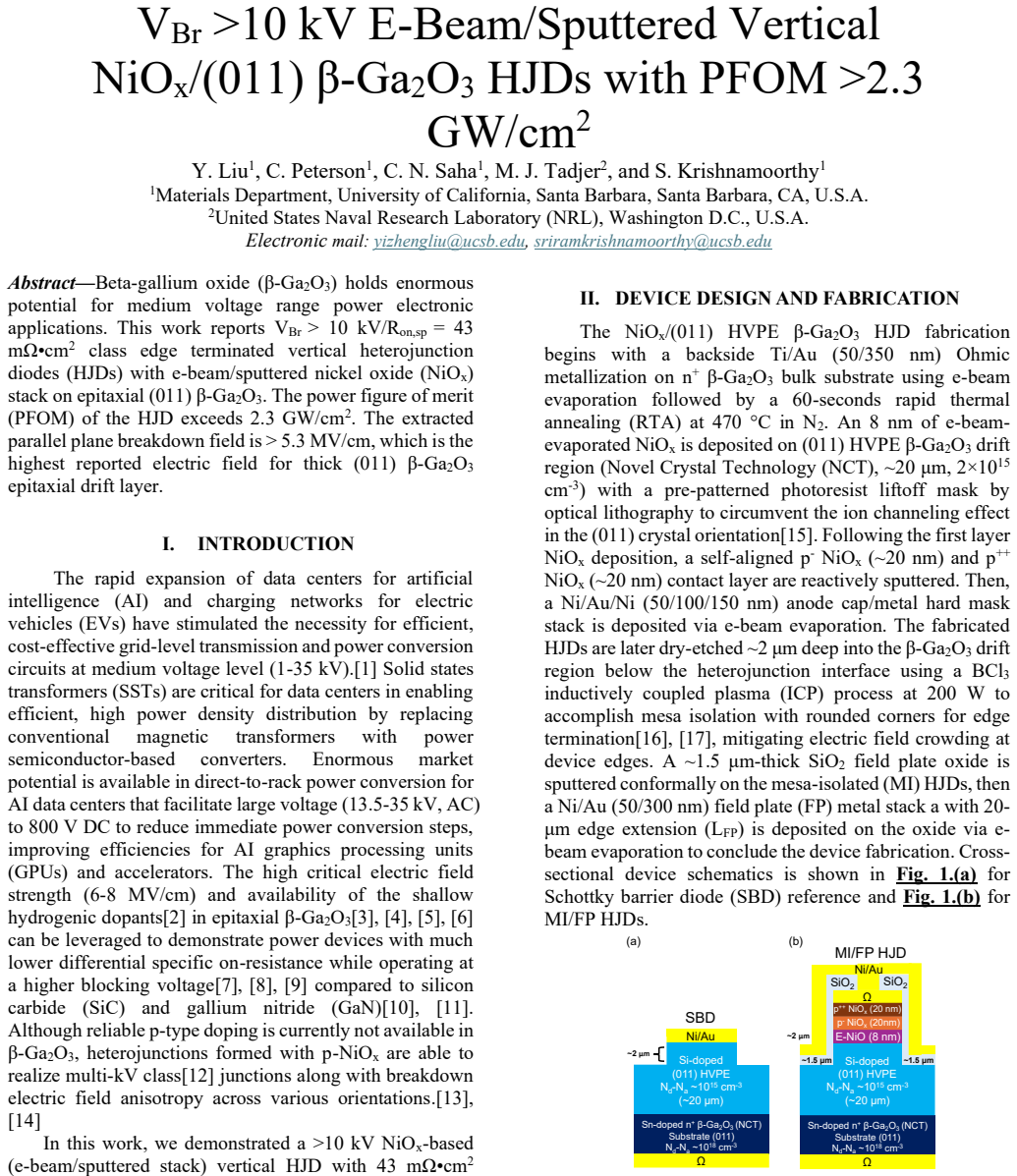
The edge termination structure combined with the nickel oxide p-type layer deposited by e-beam and sputtering on the n-type (011) β-Ga2O3, which together are designed to sustain high electric fields up to the parallel plane breakdown limit.
If this is right
- These diodes demonstrate the feasibility of vertical high-voltage devices exceeding 10 kV in beta-gallium oxide.
- The high extracted breakdown field indicates that the material can support stronger electric fields in the (011) orientation than previously achieved in thick drift layers.
- Power converters for medium voltage applications could benefit from the low on-resistance at high breakdown voltage.
- The use of a simple NiOx stack suggests a scalable fabrication approach for such high-performance devices.
Where Pith is reading between the lines
- If confirmed, this high field strength may lead to designs that optimize the (011) orientation for better device performance in power electronics.
- The result could motivate testing similar NiOx stacks on other beta-gallium oxide orientations or related materials to achieve comparable voltages.
- Further work might explore how varying the drift layer thickness affects the achievable breakdown while maintaining the figure of merit.
Load-bearing premise
The edge termination prevents any premature breakdown at the device periphery or surface, allowing the observed breakdown to occur at the full parallel-plane field strength calculated from the device geometry and doping.
What would settle it
Direct measurement of the electric field profile in the drift layer at breakdown, for example using scanning probe techniques, showing a peak field below 5.3 MV/cm would falsify the extracted parallel plane breakdown field claim.
Figures

read the original abstract
Beta-gallium oxide (\beta-Ga2O3) holds enormous potential for medium voltage range power electronic applications. This work reports VBr > 10 kV/Ron,sp = 43 m\Omega*cm2 class edge terminated vertical heterojunction diodes (HJDs) with e-beam/sputtered nickel oxide (NiOx) stack on epitaxial (011) \beta-Ga2O3. The power figure of merit (PFOM) of the HJD exceeds 2.3 GW/cm2. The extracted parallel plane breakdown field is > 5.3 MV/cm, which is the highest reported electric field for thick (011) \beta-Ga2O3 epitaxial drift layer.
Editorial analysis
A structured set of objections, weighed in public.
Referee Report
Summary. The manuscript reports fabrication of edge-terminated vertical heterojunction diodes (HJDs) using e-beam/sputtered NiOx on epitaxial (011) β-Ga2O3, achieving VBr >10 kV with Ron,sp = 43 mΩ·cm², PFOM >2.3 GW/cm², and an extracted parallel-plane breakdown field >5.3 MV/cm (claimed highest for thick (011) drift layers).
Significance. If substantiated, the result would be significant for β-Ga2O3 power electronics, demonstrating record breakdown fields in the (011) orientation alongside competitive PFOM for medium-voltage applications.
major comments (2)
- [Abstract] Abstract and results section: key metrics (VBr >10 kV, Ron,sp =43 mΩ·cm², E>5.3 MV/cm) are presented without error bars, device-to-device statistics, or measurement details, so the central performance claims cannot be evaluated for reliability or reproducibility.
- [Results and Discussion] Device characterization and discussion: the parallel-plane field extraction >5.3 MV/cm depends on assumptions of uniform doping, precise drift-layer thickness (<5% accuracy), and full suppression of edge/surface breakdown by the NiOx stack plus termination; no SIMS/C-V profiles, TCAD validation, or geometric analysis are supplied to confirm the measured VBr reflects the material limit.
minor comments (1)
- [Abstract] Notation for specific on-resistance is written as mΩ*cm2 in the abstract; standardize to mΩ·cm² throughout.
Simulated Author's Rebuttal
We thank the referee for their thorough review and constructive comments on our manuscript. We have addressed the concerns about statistical presentation and validation of the breakdown field extraction by revising the manuscript to include additional data and details. Point-by-point responses follow.
read point-by-point responses
-
Referee: [Abstract] Abstract and results section: key metrics (VBr >10 kV, Ron,sp =43 mΩ·cm², E>5.3 MV/cm) are presented without error bars, device-to-device statistics, or measurement details, so the central performance claims cannot be evaluated for reliability or reproducibility.
Authors: We agree that error bars, device-to-device statistics, and explicit measurement details are necessary to substantiate the reliability of the reported metrics. In the revised manuscript, we have added error bars to the key figures, included statistics (mean and standard deviation) from measurements on multiple devices, and expanded the methods section with full details on the high-voltage testing setup, on-resistance extraction procedure, and measurement conditions. revision: yes
-
Referee: [Results and Discussion] Device characterization and discussion: the parallel-plane field extraction >5.3 MV/cm depends on assumptions of uniform doping, precise drift-layer thickness (<5% accuracy), and full suppression of edge/surface breakdown by the NiOx stack plus termination; no SIMS/C-V profiles, TCAD validation, or geometric analysis are supplied to confirm the measured VBr reflects the material limit.
Authors: We acknowledge that the parallel-plane field extraction relies on key assumptions and that supporting data were not originally provided. In the revised manuscript, we have added C-V profiling results confirming uniform doping and drift-layer thickness accuracy within 5%, TCAD simulations validating edge termination effectiveness in suppressing premature breakdown, and a geometric analysis of the device structure demonstrating that breakdown occurs in the parallel-plane region. These additions support that the extracted field >5.3 MV/cm corresponds to the material limit. revision: yes
Circularity Check
No circularity: pure experimental device report with measured values and standard figures of merit.
full rationale
The paper reports fabricated devices, measured breakdown voltages (VBr > 10 kV), specific on-resistance (Ron,sp = 43 mΩ·cm²), and derived PFOM (> 2.3 GW/cm²) plus an extracted parallel-plane field (> 5.3 MV/cm) from I-V data on (011) β-Ga2O3 HJDs. No derivation chain, fitted parameters, self-citations of uniqueness theorems, or ansatzes are present in the provided text; all headline numbers are direct experimental outputs or simple arithmetic combinations of measured quantities. The skeptic concerns address extraction assumptions and validation gaps (doping uniformity, edge termination efficacy), which are correctness risks rather than circular reductions of the result to its own inputs. The work is therefore self-contained against external benchmarks with score 0.
Axiom & Free-Parameter Ledger
axioms (1)
- domain assumption Standard assumptions of uniform epitaxial doping and accurate extraction of parallel-plane field from terminal I-V characteristics
Reference graph
Works this paper leans on
-
[1]
High Responsivity Optically-Triggered Vertical GaN Heterojunction Power Switches With kHz Operation,
J.-H. Hsia, Z. Zhu, Y. Liu, J. Niroula, M. Oh, J. A. Perozek, J. Park, S. Krishnamoorthy, T. Palacios., “High Responsivity Optically-Triggered Vertical GaN Heterojunction Power Switches With kHz Operation,” IEEE Electron Device Lett., vol. 47, no. 3, pp. 498 – 501, Mar. 2026, doi: 10.1109/led.2026.3651209
-
[2]
Donors and deep acceptors in β -Ga2O3,
A. T. Neal, S. Mou, S. Rafique, H. Zhao, E. Ahmadi, J. S. Speck, K. T. Stevens, J. D. Blevins, D. B. Thomson, N. Moser, K. D. Chabak, G. H. Jessen, “Donors and deep acceptors in β -Ga2O3,” Applied Physics Letters , vol. 113, no. 6, Aug. 2018, doi: 10.1063/1.5034474
-
[3]
A. Bhattacharyya, C. Peterson, K. Chanchaiworawit, S. Roy, Y. Liu, S. Rebollo, S. Krishnamoorthy, “Over 6 μm thick MOCVD -grown low -background carrier density (10 15 cm−3) high-mobility (010) β -Ga2O3 drift layers,” Applied Physics Letters , vol. 124, no. 1, Jan. 2024, doi: 10.1063/5.0188773
-
[4]
C. Peterson , A. Bhattacharyya, K. Chanchaiworawit, R. Kahler, S. Roy, Y. Liu, S. Rebollo, A. Kallistova, T. E. Mates, S. Krishnamoorthy., “200 cm 2/Vs electron mobility and controlled low 10 15 cm−3 Si doping in (010) β -Ga2O3 epitaxial drift layers,” Applied Physics Letters, vol. 125, no. 18, Oct. 2024, doi: 10.1063/5.0230413
-
[5]
S. Rebollo, Y. Liu, C. Peterson, S. Krishnamoorthy, and J. S. Speck, “Growth of nitrogen -doped (010) β - Ga2O3 by plasma -assisted molecular beam epitaxy using an O2/N2 gas mixture,” Applied Physics Letters, vol. 126, no. 8, Feb. 2025, doi: 10.1063/5.0250037
-
[6]
C. Peterson, C. N. Saha, R. Kahler, Y. Liu, A. Mattapalli, S. Roy, S. Krishnamoorthy, “Kilovolt-class β-Ga2O3 field-plated Schottky barrier diodes with MOCVD-grown intentionally 10 15 cm-3 doped drift layers,” Journal of Applied Physics , vol. 138, no. 18, Nov. 2025, doi: 10.1063/5.0302735
-
[7]
S. Roy, B. Kostroun, Y. Liu, J. Cooke, A. Bhattacharyya, C. Peterson, B. S. Rodriguez, S. Krishnamoorthy, “Low Q CVF 20 A/1.4 kV β -Ga₂O₃ Vertical Trench High -k RESURF Schottky Barrier Diode With Turn-On Voltage of 0.5 V,” IEEE Electron Device Lett. , vol. 45, no. 12, pp. 2487 –2490, Sep. 2024, doi: 10.1109/led.2024.3469283
-
[8]
S. Roy, B. Kostroun, J. Cooke, Y. Liu, A. Bhattacharyya, C. Peterson, B. S. Rodriguez, S. Krishnamoorthy, “Ultra -low reverse leakage in large area kilo -volt class β -Ga2O3 trench Schottky barrier diode with high -k dielectric RESURF,” Applied Physics Letters , vol. 123, no. 24, Dec. 2023, doi: 10.1063/5.0175674
-
[9]
2.34 kV β -Ga2O3 vertical trench RESURF Schottky barrier diode with sub -micron fin width,
C. N. Saha, S. Roy, Y. Liu, C. Peterson, and S. Krishnamoorthy, “2.34 kV β -Ga2O3 vertical trench RESURF Schottky barrier diode with sub -micron fin width,” APL Electronic Devices , vol. 1, no. 4, Dec. 2025, doi: 10.1063/5.0299732
-
[10]
Y. Zhang and J. S. Speck, “Importance of shallow hydrogenic dopants and material purity of ultra -wide bandgap semiconductors for vertical power electron devices,” Semicond. Sci. Technol ., vol. 35, no. 12, p. 125018, Oct. 2020, doi: 10.1088/1361-6641/abbba6
-
[11]
B. J. Baliga, Fundamentals of power semiconductor devices. Springer Science & Business Media, 2010
2010
-
[12]
Breakdown up to 13.5 kV in NiO/β -Ga2O3 Vertical Heterojunction Rectifiers,
J.-S. Li, H. H. Wan, C. C. Chiang, T. J. Yoo, M. H. Yu, F. Ren, H. Kim, Y. T Liao and S. J. Pearton, “Breakdown up to 13.5 kV in NiO/β -Ga2O3 Vertical Heterojunction Rectifiers,” ECS J. Solid State Sci. Technol., vol. 13, no. 3, p. 035003, Mar. 2024, doi: 10.1149/2162-8777/ad3457
-
[13]
Orientation -dependent β -Ga2O3 heterojunction diode with atomic layer deposition (ALD) NiO,
Y. Liu, S. M. W. Witsell, J. F. Conley Jr., and S. Krishnamoorthy, “Orientation -dependent β -Ga2O3 heterojunction diode with atomic layer deposition (ALD) NiO,” Applied Physics Letters, vol. 127, no. 12, Sep. 2025, doi: 10.1063/5.0285622
-
[14]
Y. Liu, H. Wang, C. Peterson, J. S. Speck, C. V. D. Walle, and S. Krishnamoorthy, “Cr 2O3/β-Ga2O3 Heterojunction Diodes with Orientation -Dependent Breakdown Electric Field up to 12.9 MV/cm,” ArXiv Nov. 25, 2025 , A rXiv:2511.20885. doi: 10.48550/arXiv.2511.20885
-
[15]
Evidence of Micron-Scale Ion Damage in (010), (110), and (011) ${\beta}-Ga_2O_3$ Epitaxial Layers
C. Peterson, C. N. Saha, Y. Liu, J. S. Speck, and S. Krishnamoorthy, “Evidence of Micron -Scale Ion Damage in (010), (110), and (011) β-Ga2O3 Epitaxial Layers,” Apr. 27, 2026, ArXiv: arXiv:2604.24190. doi: 10.48550/arXiv.2604.24190
work page internal anchor Pith review Pith/arXiv arXiv doi:10.48550/arxiv.2604.24190 2026
-
[16]
3.3 kV -class NiO/β-Ga2O3 heterojunction diode and its off -state leakage mechanism,
J. Wan, H. Wang, C. Zhang, Y. Li, C. Wang, H. Cheng, J. Li, N. Ren, Q. Guo, K. Sheng “3.3 kV -class NiO/β-Ga2O3 heterojunction diode and its off -state leakage mechanism,” Applied Physics Letters , vol. 124, no. 24, Jun. 2024, doi: 10.1063/5.0211183
-
[17]
Y. Liu, S. Roy, C. Peterson, A. Bhattacharyya, and S. Krishnamoorthy, “Ultra -low reverse leakage NiOx/β - Ga2O3 heterojunction diode achieving breakdown voltage >3 kV with plasma etch field -termination,” AIP Advances , vol. 15, no. 1, Jan. 2025, doi: 10.1063/5.0251069
-
[18]
2.1 kV (001) -β-Ga2O3 vertical Schottky barrier diode with high -k oxide field plate,
S. Roy, A. Bhattacharyya, C. Peterson, and S. Krishnamoorthy, “2.1 kV (001) -β-Ga2O3 vertical Schottky barrier diode with high -k oxide field plate,”Applied Physics Letters , vol. 122, no. 15, Apr. 2023, doi: 10.1063/5.0137935
-
[19]
NiO junction termination extension for high -voltage (> 3 kV) Ga2O3 devices,
M. Xiao, B. Wang, J. Spencer, Y. Qin, M. Porter, Y. Ma, Y. Wang, K. Sasaki, M. Tadjer, Y. Zhang, “NiO junction termination extension for high -voltage (> 3 kV) Ga2O3 devices,” Applied Physics Letters, vol. 122, no. 18, May 2023, doi: 10.1063/5.0142229
-
[20]
X. Lu, X. Zhou, H. Jiang, K. W. Ng, Z. Chen, Y. Pei, K. M. Lau, G. Wang “1 -kV Sputtered p-NiO/n-Ga2O3 Heterojunction Diodes With an Ultra -Low Leakage Current Below 1 μA/cm2,” IEEE Electron Device Lett., vol. 41, no. 3, pp. 449 –452, Mar. 2020, doi: 10.1109/led.2020.2967418
-
[21]
A 1.86-kV double-layered NiO/β-Ga2O3 vertical p –n heterojunction diode,
H. H. Gong, X. H. Chen, Y. Xu, F. -F. Ren, S. L. Gu, and J. D. Ye, “A 1.86-kV double-layered NiO/β-Ga2O3 vertical p –n heterojunction diode,” Applied Physics Letters, vol. 117, no. 2, Jul. 2020, doi: 10.1063/5.0010052
-
[22]
F. Zhou, F. Zhou, H. Gong, W. Xu, X. Yu, Y. Xu, Y. Yang, F. Ren, S. Gu, Y. Zheng, R. Zhang, J. Ye, H. Lu., “1.95 -kV Beveled -Mesa NiO/β -Ga2O3 Heterojunction Diode With 98.5% Conversion Efficiency and Over Million -Times Overvoltage Ruggedness,” I EEE Trans. Power Electron ., vol. 37, no. 2, pp. 1223 –1227, Feb. 2022, doi: 10.1109/tpel.2021.3108780
-
[23]
Y. Wang, Y. Wang, H. Gong, Y. Lv, X. Fu, S. Dun, T. Han, H. Liu, X. Zhou, S. Liang, J. Ye, R. Zhang, A. Bu, S. Cai, Z. Feng, “2.41 kV Vertical P-Nio/n-Ga2O3 Heterojunction Diodes With a Record Baliga’s Figure- of-Merit of 5.18 GW/cm 2,” IEEE Trans. Power Electron., vol. 37, no. 4, pp. 3743 –3746, Apr. 2022, doi: 10.1109/tpel.2021.3123940
-
[24]
7.5 kV, 6.2 GW cm −2 NiO/β-Ga2O3 vertical rectifiers with on –off ratio greater than 10 13,
J.-S. Li, C.-C. Chiang, X. Xia, H.-H. Wan, F. Ren, and S. J. Pearton, “7.5 kV, 6.2 GW cm −2 NiO/β-Ga2O3 vertical rectifiers with on –off ratio greater than 10 13,” Journal of Vacuum Science & Technology A , vol. 41, no. 3, Apr. 2023, doi: 10.1116/6.0002580
-
[25]
NiO/Ga 2O3 Vertical Rectifiers of 7 kV and 1 mm 2 with 5.5 A Forward Conduction Current,
J.-S. Li, H. H. Wan, C. C. Chiang, T. J. Yoo, F. Ren, H. Kim, S. J. Pearton, “NiO/Ga 2O3 Vertical Rectifiers of 7 kV and 1 mm 2 with 5.5 A Forward Conduction Current,” Crystals, vol. 13, no. 12, p. 1624, Nov. 2023, doi: 10.3390/cryst13121624
discussion (0)
Sign in with ORCID, Apple, or X to comment. Anyone can read and Pith papers without signing in.