Recognition: 2 theorem links
· Lean TheoremMonolithic 3D Integration for Null Convention Logic (NCL)-Based Asynchronous Circuits
Pith reviewed 2026-05-08 18:55 UTC · model grok-4.3
The pith
Monolithic 3D integration applied to Null Convention Logic reduces area by 44 percent while also lowering delay and power.
A machine-rendered reading of the paper's core claim, the machinery that carries it, and where it could break.
Core claim
Stacking NCL threshold gates across monolithic 3D layers produces an unsigned array multiplier whose simulated area is 44 percent smaller than its 2D counterpart, with corresponding reductions in delay of 31 percent and power of 17 percent, when only a conservative wirelength benefit is credited to the vertical integration.
What carries the argument
The M3D-NCL standard-cell design methodology that places threshold gates in vertically stacked layers to shorten interconnects while retaining the quasi-delay-insensitive behavior of NCL.
If this is right
- NCL-based asynchronous circuits become viable for area-constrained applications once their footprint is reduced by nearly half.
- The same stacking approach can be applied to other quasi-delay-insensitive asynchronous blocks beyond multipliers.
- Power and speed advantages of asynchronous designs become more attainable when area overhead is mitigated by vertical integration.
- Standard-cell libraries for NCL can be extended to M3D processes without altering the fundamental threshold-gate logic.
Where Pith is reading between the lines
- Widespread use of this method would require new place-and-route tools that account for vertical vias and layer-specific parasitics in asynchronous timing analysis.
- The area savings could make NCL attractive for battery-powered or thermally limited devices where clock distribution costs are high.
- Testing the approach on larger circuits such as processors or filters would reveal whether the reported gains scale beyond the multiplier example.
Load-bearing premise
That monolithic 3D stacking yields a net wirelength reduction without adding parasitic effects, thermal gradients, or manufacturing defects large enough to erase the reported area, delay, and power improvements.
What would settle it
A physical prototype of the M3D-NCL multiplier fabricated in an actual monolithic 3D process whose measured area, delay, and power are compared against the simulation results that assumed only conservative wirelength savings.
Figures

read the original abstract
As the demand for high-speed and low-power electronics continues to grow, the quasi-delay-insensitive (QDI) asynchronous domain of digital design has emerged as a promising alternative to traditional clock-based designs. However, the adoption of the paradigm has been greatly limited due to the lack of mature computer-aided design (CAD) tools and a substantially larger area footprint, owing to various architectural constraints. Monolithic-3D (M3D) technology has recently paved the way for manufacturing highly dense integrated circuits (ICs) through sequential integration, resulting in a reduced area footprint, shorter wirelengths, and increased performance. In this study, we integrate M3D technology with QDI Null Convention Logic (NCL) and propose a design methodology for the implementation of M3D-based NCL standard cells, aimed at mitigating the area inefficiencies of traditional planar or 2D counterparts. Furthermore, we employed the threshold gates to design an M3D-NCL unsigned array multiplier circuit. Simulation results suggest that, for a conservative wirelength reduction resulting from M3D implementation, a substantial area reduction of 44% can be achieved while simultaneously reducing delay and power by approximately 31% and 17%, respectively.
Editorial analysis
A structured set of objections, weighed in public.
Referee Report
Summary. The manuscript proposes a design methodology for Monolithic 3D (M3D) integration of Null Convention Logic (NCL) standard cells to reduce the area footprint of quasi-delay-insensitive asynchronous circuits. It demonstrates the approach on an unsigned array multiplier and reports simulation results of 44% area reduction, 31% delay reduction, and 17% power reduction under a conservative wirelength reduction assumption arising from M3D stacking.
Significance. If the quantitative claims can be substantiated with explicit M3D parasitic and thermal models, the work would offer a concrete path to mitigating the well-known area penalty of NCL/QDI designs while preserving their timing robustness, which could accelerate adoption in low-power, high-reliability domains. The cell-level methodology itself constitutes a targeted, reusable contribution at the intersection of asynchronous logic and sequential 3D integration.
major comments (2)
- [Abstract / Simulation Results] Abstract and Simulation Results section: the reported 44% area, 31% delay, and 17% power improvements rest on an unquantified 'conservative wirelength reduction' that is neither derived from NCL threshold-gate placement rules nor from measured 2D routing statistics; without the exact factor or its justification, the numerical claims cannot be independently reproduced or stress-tested.
- [Methodology / Simulation Setup] Methodology and Simulation Setup: the evaluation omits monolithic via series resistance, inter-tier coupling capacitance, and vertical thermal gradients. Because NCL employs dual-rail signaling and threshold gates whose delay is sensitive to interconnect parasitics, these omitted effects constitute a load-bearing modeling gap that could materially alter the claimed gains.
minor comments (1)
- [Abstract] The abstract refers to 'various architectural constraints' limiting NCL adoption without enumerating them; a short parenthetical list would improve accessibility for readers outside the asynchronous-design community.
Simulated Author's Rebuttal
We thank the referee for the constructive and detailed comments. We have revised the manuscript to address the concerns regarding quantification of assumptions and explicit discussion of modeling limitations. Point-by-point responses follow.
read point-by-point responses
-
Referee: [Abstract / Simulation Results] Abstract and Simulation Results section: the reported 44% area, 31% delay, and 17% power improvements rest on an unquantified 'conservative wirelength reduction' that is neither derived from NCL threshold-gate placement rules nor from measured 2D routing statistics; without the exact factor or its justification, the numerical claims cannot be independently reproduced or stress-tested.
Authors: We agree that the wirelength reduction factor must be quantified for reproducibility. The revised manuscript now explicitly states in the abstract and Simulation Results section that a conservative 25% average wirelength reduction is assumed. This value is justified as a pessimistic estimate drawn from typical M3D wirelength improvements reported in the literature for comparable logic blocks (often 30-50%), adjusted downward to account for NCL-specific dual-rail routing overhead without claiming direct derivation from our own 2D placement statistics. A short explanatory sentence has been added to the methodology to clarify the basis of the assumption. revision: yes
-
Referee: [Methodology / Simulation Setup] Methodology and Simulation Setup: the evaluation omits monolithic via series resistance, inter-tier coupling capacitance, and vertical thermal gradients. Because NCL employs dual-rail signaling and threshold gates whose delay is sensitive to interconnect parasitics, these omitted effects constitute a load-bearing modeling gap that could materially alter the claimed gains.
Authors: We concur that these parasitic and thermal effects are important and were not modeled. The revised Simulation Setup section now explicitly lists the omissions (via resistance, inter-tier coupling, and thermal gradients) as study limitations. We note that the conservative wirelength reduction was selected in part to provide margin against unmodeled parasitic penalties. Full extraction of these effects would require a complete M3D process design kit and thermal simulation infrastructure that was unavailable for the 45 nm node used here. The paper now includes a forward-looking statement on incorporating such models in follow-on work. revision: partial
Circularity Check
No significant circularity detected
full rationale
The paper's central claims rest on simulation outcomes conditioned on an explicitly stated external input ('conservative wirelength reduction resulting from M3D implementation'). This assumption is presented as a modeling choice rather than derived from the NCL threshold-gate equations or prior results within the paper. No self-definitional loops, fitted parameters renamed as predictions, or load-bearing self-citations appear in the abstract or described methodology. The reported area/delay/power figures are therefore outputs of the simulation under the given input and do not reduce to the input by construction.
Axiom & Free-Parameter Ledger
free parameters (1)
- conservative wirelength reduction
axioms (1)
- domain assumption Monolithic 3D integration reduces effective wirelength and area footprint relative to planar 2D layouts for the same logic function
Reference graph
Works this paper leans on
-
[1]
Monolithic 3D Integration for Null Convention Logic (NCL)-Based Asynchronous Circuits,
We propose the first -ever design and analysis method - ology for M3D- based implementations of static NCL (M3D-NCL) threshold gates. 2026 IEEE. Personal use of this material is permitted. Permission from IEEE must be obtained for all other uses, in any current or future media, including reprinting/republishing this material for advertising or promotional...
2026
-
[2]
We evaluate the power, performance, and area (PPA) metrics of M3D -NCL standard gates and compare those to their corresponding 2D implementations
-
[3]
We employ the M3D- NCL gates to design an unsigned NCL array multiplier to study the benefits of M3D implementation in comparison to conventional 2D im - plementation for large-scale circuits
-
[4]
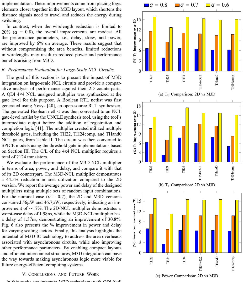
Simulation results for the NCL gates suggest that, for a conservative wirelength reduction resulting from M3D implementation, a substantial area reduction of 44% on average can be achieved while simultaneously reducing the average delay, skew, and power of the NCL gates by 10.5%, 10.2%, and 10.3%, respectively
-
[5]
The organization of the rest of the paper is as follows: Section II provides the background and related works of the current study
Simulation results for the multiplier design suggest that the M3D version outperformed the 2D version in all categories while utilizing half the area. The organization of the rest of the paper is as follows: Section II provides the background and related works of the current study. Section III discusses the proposed methodology to design and analyze the M...
-
[6]
The Node-to-Node connects the active regions of PMOS and NMOS devices
The VDD-to-Node and Node -to-GND connection scenario interconnects power rails such as VDD and GND to the transistor devices’ active regions (i.e., the source and drain). The Node-to-Node connects the active regions of PMOS and NMOS devices. The Input -to-Node connects the inputs, such as a, b, c, and d , to the gate regions of the devices. RC parasitics,...
2052
-
[7]
NULL Convention Logic/sup TM/: a complete and consistent logic for asynchronous digital circuit synthesis,
K. Fant and S. Brandt, “NULL Convention Logic/sup TM/: a complete and consistent logic for asynchronous digital circuit synthesis,” in Pro - ceedings of International Conference on Application Specific Systems, Architectures and Processors: ASAP ’96, 1996, pp. 261–273
1996
-
[8]
Smith and J
S. Smith and J. Di, Designing asynchronous circuits using NULL convention logic (NCL). Springer Nature, 2022
2022
-
[9]
Di and S
J. Di and S. C. Smith, Asynchronous Circuit Applications . Institution of Engineering and Technology, 2019
2019
-
[10]
Hardware trojan design and detection in asynchronous ncl circuits,
K. K. Ponugoti, S. K. Srinivasan, and S. C. Smith, “Hardware trojan design and detection in asynchronous ncl circuits,” in 2020 27th IEEE International Conference on Electronics, Circuits and Systems (ICECS). IEEE, 2020, pp. 1–4
2020
-
[11]
Illegal trojan design and detection in asynchronous null convention logic and sleep convention logic circuits,
K. K. Ponugoti, S. K. Srinivasan et al. , “Illegal trojan design and detection in asynchronous null convention logic and sleep convention logic circuits,” IET Computers & Digital Techniques, vol. 16, no. 5-6, pp. 172–182, 2022
2022
-
[12]
A PPA study for heterogeneous 3 -D IC options: Monolithic, hybrid bonding, and microbumping,
J. Kim, L. Zhu et al. , “A PPA study for heterogeneous 3 -D IC options: Monolithic, hybrid bonding, and microbumping,” IEEE Transactions on Very Large Scale Integration (VLSI) Systems, vol. 32, no. 3, pp. 401–412, 2023
2023
-
[13]
Efficient Metal Inter-Layer Via Utilization Strategies for Three-dimensional Integrated Circuits,
U. R. Tida and M. S. Vemuri, “Efficient Metal Inter-Layer Via Utilization Strategies for Three-dimensional Integrated Circuits,” in 2020 IEEE 33rd International System-on-Chip Conference (SOCC), 2020, pp. 195–200
2020
-
[14]
Dual- Purpose Metal Inter -layer Via Utilization in Monolithic Three- Dimensional (M3D) Integration,
M. S. Vemuri and U. Rao Tida, “Dual- Purpose Metal Inter -layer Via Utilization in Monolithic Three- Dimensional (M3D) Integration,” in 2020 IEEE 63rd International Midwest Symposium on Circuits and Systems (MWSCAS), 2020, pp. 424–427
2020
-
[15]
Evolution of NULL Convention Logic Based Asynchronous Paradigm: An Overview and Outlook,
D. Khodosevych and A. A. Sakib, “Evolution of NULL Convention Logic Based Asynchronous Paradigm: An Overview and Outlook,” IEEE Access, vol. 10, pp. 78 650–78 666, 2022
2022
-
[16]
High -density integration of functional modules using monolithic 3D -IC technology,
S. Panth, K. Samadi et al. , “High -density integration of functional modules using monolithic 3D -IC technology,” in 2013 18th Asia and South Pacific Design Automation Conference (ASP-DAC). IEEE, 2013, pp. 681–686
2013
-
[17]
Design and CAD methodologies for low power gate- level monolithic 3D ICs,
S. A. Panth, K. Samadi et al., “Design and CAD methodologies for low power gate- level monolithic 3D ICs,” in Proceedings of the 2014 international symposium on Low power electronics and design, 2014, pp. 171–176
2014
-
[18]
Ultrahigh density logic designs using mono - lithic 3-D integration,
Y.-J. Lee and S. K. Lim, “Ultrahigh density logic designs using mono - lithic 3-D integration,” IEEE Transactions on Computer-Aided Design of Integrated Circuits and Systems, vol. 32, no. 12, pp. 1892–1905, 2013
1905
-
[19]
Mono3D: Open Source Cell Library for Monolithic 3-D Integrated Circuits,
C. Yan and E. Salman, “Mono3D: Open Source Cell Library for Monolithic 3-D Integrated Circuits,” IEEE Transactions on Circuits and Systems I: Regular Papers, vol. 65, no. 3, pp. 1075–1085, 2018
2018
-
[20]
Opportunities brought by sequential 3D CoolCube™ integration,
M. Vinet, P. Batude et al. , “Opportunities brought by sequential 3D CoolCube™ integration,” in 2016 46th European Solid- State Device Research Conference (ESSDERC). IEEE, 2016, pp. 226–229
2016
-
[21]
Low temperature and ion -cut based monolithic 3D process integration platform incorporated with CMOS, RRAM and photo-sensor circuits,
H. Han, R. Choi et al. , “Low temperature and ion -cut based monolithic 3D process integration platform incorporated with CMOS, RRAM and photo-sensor circuits,” in 2020 IEEE International Electron Devices Meeting (IEDM). IEEE, 2020, pp. 15–6
2020
-
[22]
Low thermal budget processing for sequential 3-D IC fabrication,
B. Rajendran, R. S. Shenoy et al. , “Low thermal budget processing for sequential 3-D IC fabrication,” IEEE Transactions on Electron Devices, vol. 54, no. 4, pp. 707–714, 2007
2007
-
[23]
Transistor-level monolithic 3D standard cell layout optimization for full- chip static power integrity,
B. W. Ku, T. Song et al., “Transistor-level monolithic 3D standard cell layout optimization for full- chip static power integrity,” in 2017 IEEE/ACM International Symposium on Low Power Electronics and Design (ISLPED). IEEE, 2017, pp. 1–6
2017
-
[24]
Modeling and Design of Dual- purpose MIV in Monolithic 3D IC,
M. S. Vemuri and U. R. Tida, “Modeling and Design of Dual- purpose MIV in Monolithic 3D IC,” IEEE Access, 2024
2024
-
[25]
Compact 6T- SRAM using bottom-gate transistor in FD -SOI process for Monolithic- 3D Integra - tion,
M. S. Vemuri, T. Ahmed, and U. R. Tida, “Compact 6T- SRAM using bottom-gate transistor in FD -SOI process for Monolithic- 3D Integra - tion,” in 2024 IEEE Computer Society Annual Symposium on VLSI (ISVLSI). IEEE, 2024, pp. 725–729
2024
-
[26]
Design of asynchronous circuits by synchronous CAD tools,
A. Kondratyev and K. Lwin, “Design of asynchronous circuits by synchronous CAD tools,” in Proceedings of the 39th annual Design Automation Conference, 2002, pp. 411–414
2002
-
[27]
Optimization of robust asynchronous circuits by local input completeness relaxation,
C. Jeong and S. M. Nowick, “Optimization of robust asynchronous circuits by local input completeness relaxation,” in 2007 Asia and South Pacific Design Automation Conference. IEEE, 2007, pp. 622–627
2007
-
[28]
Block -level relaxation for timing -robust asynchronous circuits based on eager evaluation,
——, “Block -level relaxation for timing -robust asynchronous circuits based on eager evaluation,” in 2008 14th IEEE International Symposium on Asynchronous Circuits and Systems. IEEE, 2008, pp. 95–104
2008
-
[29]
ASCEND: Advanced Synthesis, Circuit Exploration, and Design Optimization for NCL Circuits,
A. Bodoh and A. A. Sakib, “ASCEND: Advanced Synthesis, Circuit Exploration, and Design Optimization for NCL Circuits,” in 2024 31st IEEE International Conference on Electronics, Circuits and Systems (ICECS), 2024, pp. 1–4
2024
-
[30]
CMOS implementation of static threshold gates with hysteresis: A new approach,
F. A. Parsan and S. C. Smith, “CMOS implementation of static threshold gates with hysteresis: A new approach,” in 2012 IEEE/IFIP 20th Inter - national Conference on VLSI and System -on-Chip (VLSI -SoC). IEEE, 2012, pp. 41–45
2012
-
[31]
Static Differential NCL Gates: Toward Low Power,
M. T. Moreira, M. Arendt et al., “Static Differential NCL Gates: Toward Low Power,” IEEE Transactions on Circuits and Systems II: Express Briefs, vol. 62, no. 6, pp. 563–567, 2015
2015
-
[32]
Comprehensive Comparison of NULL Convention Logic Threshold Gate Implementations,
K. Haulmark, W. Khalil et al. , “Comprehensive Comparison of NULL Convention Logic Threshold Gate Implementations,” in 2018 New Generation of CAS (NGCAS), 2018, pp. 37–40
2018
-
[33]
Implementation of Static NCL Threshold Gates Using Emerging CNTFET Technology,
A. A. Sakib and S. C. Smith, “Implementation of Static NCL Threshold Gates Using Emerging CNTFET Technology,” in 2020 27th IEEE International Conference on Electronics, Circuits and Systems (ICECS), 2020, pp. 1–4
2020
-
[34]
Implementation of FinFET Based Static NCL Threshold Gates: An Analysis of Design Choice,
A. A. Sakib, A. A. Akib, and S. C. Smith, “Implementation of FinFET Based Static NCL Threshold Gates: An Analysis of Design Choice,” in 2020 IEEE 63rd International Midwest Symposium on Circuits and Systems (MWSCAS), 2020, pp. 37–40
2020
-
[35]
Clockless spintronic logic: A robust and ultra-low power computing paradigm,
Y. Bai, R. F. DeMara et al., “Clockless spintronic logic: A robust and ultra-low power computing paradigm,” IEEE Transactions on Comput - ers, vol. 67, no. 5, pp. 631–645, 2017
2017
-
[36]
Sabado II, Asynchronous 3D (Async3D): Design Methodology and Analysis of 3D Asynchronous Circuits
F. Sabado II, Asynchronous 3D (Async3D): Design Methodology and Analysis of 3D Asynchronous Circuits. University of Arkansas, 2017
2017
-
[37]
Monolithic 3D IC vs. TSV-based 3D IC in 14nm FinFET technology,
S. K. Samal, D. Nayak et al., “Monolithic 3D IC vs. TSV-based 3D IC in 14nm FinFET technology,” in 2016 IEEE SOI -3D-Subthreshold Microelectronics Technology Unified Conference (S3S). IEEE, 2016, pp. 1–2
2016
-
[38]
Low power monolithic 3D IC design of asynchronous AES core,
N. L. Penmetsa, C. Sotiriou, and S. K. Lim, “Low power monolithic 3D IC design of asynchronous AES core,” in 2015 21st IEEE International Symposium on Asynchronous Circuits and Systems . IEEE, 2015, pp. 93–99
2015
-
[39]
(2025) FreePDK45 - 45nm Open-Source PDK
NC State University. (2025) FreePDK45 - 45nm Open-Source PDK. Accessed: 2025 -05-21. [Online]. Available: https://eda.ncsu.edu/ freepdk/freepdk45/
2025
-
[40]
FDSOI Process Based MIV -transistor Utilization for Standard Cell Designs in Monolithic 3D Integration,
M. S. Vemuri and U. Rao Tida, “FDSOI Process Based MIV -transistor Utilization for Standard Cell Designs in Monolithic 3D Integration,” in 2023 IEEE 36th International System -on-Chip Conference (SOCC) , 2023, pp. 1–6
2023
-
[41]
Three -dimensional integrated circuits,
A. W. Topol, D. C. L. Tulipe et al. , “Three -dimensional integrated circuits,” IBM Journal of Research and Development, vol. 50, no. 4.5, pp. 491–506, 2006
2006
-
[42]
Metal Inter-layer Via Keep-out-zone in M3D IC: A Critical Process -aware Design Consideration,
M. S. Vemuri and U. R. Tida, “Metal Inter-layer Via Keep-out-zone in M3D IC: A Critical Process -aware Design Consideration,” in 24th International Symposium on Quality Electronic Design (ISQED). IEEE, 2023, pp. 1–8
2023
-
[43]
An analysis of the effect of wire resistance on circuit level performance at the 45-nm technology node,
V. Nguyen, P. Christie et al., “An analysis of the effect of wire resistance on circuit level performance at the 45-nm technology node,” 07 2005, pp. 191 – 193
2005
-
[44]
Asynchronous logics and application to information processing,
D. E. Muller, “Asynchronous logics and application to information processing,” in Symposium on the Application of Switching Theory to Space Technology. Stanford University Press, 1962, pp. 289–297
1962
-
[45]
Ultra high density logic designs using transistor-level monolithic 3D integration,
Y.-J. Lee, P. Morrow, and S. K. Lim, “Ultra high density logic designs using transistor-level monolithic 3D integration,” in Proceedings of the International Conference on Computer -Aided Design , 2012, pp. 539– 546
2012
-
[46]
Yosys Open SYnthesis Suite,
C. Wolf, “Yosys Open SYnthesis Suite,” https://yosyshq.net/yosys/
-
[47]
Uncle—Unified NCL Environment—an NCL design tool
R. A. Taylor and R. B. Reese, “Uncle—Unified NCL Environment—an NCL design tool.” IET, 2019
2019
discussion (0)
Sign in with ORCID, Apple, or X to comment. Anyone can read and Pith papers without signing in.