Recognition: 2 theorem links
· Lean TheoremInsights into the Nature of Quantum Emitters in Electron-Irradiated hexagonal Boron Nitride
Pith reviewed 2026-05-14 19:51 UTC · model grok-4.3
The pith
Electron irradiation of hBN produces intrinsic quantum emitters stable in layers thinner than 10 nm, distinct from organic contaminants.
A machine-rendered reading of the paper's core claim, the machinery that carries it, and where it could break.
Core claim
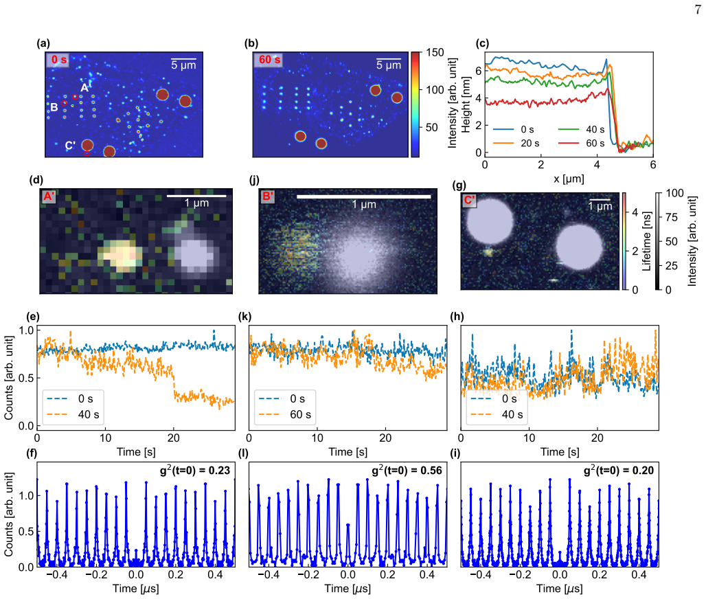
The central claim is that the green-yellow emitters in electron-irradiated hBN are intrinsic defects created by the irradiation, not organic contaminants. This is shown by their persistence after thermal annealing and oxygen plasma etching in samples prepared without any additional steps, together with hyperspectral maps that locate the emission inside the material. The work also documents spectral variability, thermal stability, and vertical localization within the hBN, and confirms that stable emitters can be formed in flakes thinner than 10 nm.
What carries the argument
A step-by-step experimental sequence of hyperspectral imaging for spectral and spatial mapping, thermal annealing for stability testing, and oxygen plasma etching for surface sensitivity that distinguishes intrinsic irradiation-induced defects from surface contaminants.
If this is right
- Emitter generation can be controlled by electron irradiation alone without extra processing steps.
- Stable single-photon sources become available in atomically thin hBN for 2D photonic devices.
- Reproducibility improves once attention shifts from contamination artifacts to irradiation-induced defects.
- Spectral variability must be characterized and managed for consistent device performance.
- Thermal stability allows operation of these emitters at elevated temperatures in practical setups.
Where Pith is reading between the lines
- The same differentiation sequence could be used to identify intrinsic emitters in other electron-irradiated 2D materials.
- Compatibility with sub-10 nm flakes suggests these emitters can be placed inside van der Waals heterostructures.
- Varying irradiation dose or energy while repeating the tests could map additional defect species.
- The framework offers a template for excluding preparation artifacts across quantum-emitter studies in layered materials.
Load-bearing premise
Thermal annealing and oxygen plasma etching affect organic contaminants differently from intrinsic hBN defects without the treatments themselves creating or destroying emitters in ways that mimic the expected contaminant pattern.
What would settle it
Finding that emitters in deliberately contaminated but non-irradiated hBN samples exhibit the same thermal stability and resistance to plasma etching as the irradiated samples, or that irradiated emitters disappear exactly when contaminants would, would falsify the intrinsic-defect claim.
Figures


read the original abstract
Quantum emitters in hexagonal boron nitride (hBN) have emerged as a promising solid-state platform for quantum technology applications. However, a persistent challenge in the field is the unclear origin of many observed emission lines, particularly in the visible range, which can be difficult to distinguish from signals arising from organic or process-induced contamination during sample preparations and handling. This ambiguity limits both the reproducibility of emitter generation and the reliable identification of truly intrinsic quantum defects. This work provides a step-by-step framework to assess whether quantum emitters in electron-irradiated hBN are associated with organic contaminants introduced during sample preparation. We employ hyperspectral imaging, thermal annealing, and oxygen plasma etching to investigate the origin of the green-yellow emitters in electron-irradiated hBN. The combined results not only rule out organic contamination as the source of emission but also provide insight into the spectral variability, thermal stability, and vertical localization of the emitters generated in electron-irradiated hBN that was created without any pre- or post-processing. In addition, our experiments demonstrate the feasibility of creating stable emitters in hBN with thicknesses below 10 nm. These findings provide practical guidance for the identification and controlled implementation of hBN-based single-photon emitters in quantum photonic devices.
Editorial analysis
A structured set of objections, weighed in public.
Referee Report
Summary. The manuscript reports an experimental investigation of green-yellow quantum emitters in electron-irradiated hexagonal boron nitride (hBN) prepared without pre- or post-processing. Using hyperspectral imaging before and after thermal annealing and oxygen plasma etching, the authors conclude that the emitters are intrinsic defects rather than organic contaminants, while also characterizing their spectral variability, thermal stability, and vertical localization; they further demonstrate stable emission in hBN flakes thinner than 10 nm.
Significance. If the differential response to annealing and etching reliably distinguishes intrinsic defects, the work supplies a practical protocol for identifying genuine hBN emitters and supports their use in ultrathin layers, both of which would aid reproducibility in quantum-photonic applications.
major comments (1)
- The central claim that organic contamination is excluded rests on the differential persistence of emitters under thermal annealing and oxygen plasma etching. The manuscript should explicitly address whether these treatments were applied to non-irradiated control samples to confirm that they neither create nor destroy intrinsic emitters in a way that could mimic the observed contaminant-free behavior.
minor comments (2)
- The abstract and methods would benefit from a brief statement of the number of flakes examined and the statistical criteria used to classify emitters as stable or unstable after treatment.
- Figure captions describing hyperspectral maps should include the excitation wavelength and collection bandwidth to allow direct comparison with other hBN studies.
Simulated Author's Rebuttal
We thank the referee for their positive assessment of our work and for the constructive suggestion. We address the single major comment below and have revised the manuscript accordingly.
read point-by-point responses
-
Referee: The central claim that organic contamination is excluded rests on the differential persistence of emitters under thermal annealing and oxygen plasma etching. The manuscript should explicitly address whether these treatments were applied to non-irradiated control samples to confirm that they neither create nor destroy intrinsic emitters in a way that could mimic the observed contaminant-free behavior.
Authors: We agree that explicit control experiments strengthen the interpretation. In the revised manuscript we have added a dedicated subsection (new Figure S3 and accompanying text in Section 3.2) reporting results from non-irradiated hBN flakes subjected to identical thermal annealing (up to 800 °C) and oxygen plasma etching protocols. These control samples showed no emergence of green-yellow emitters either before or after treatment, while the irradiated samples retained the same emitter population after annealing and only a modest reduction after etching. This differential behavior confirms that the treatments themselves neither create nor selectively destroy the observed emitters, supporting our conclusion that the emitters originate from irradiation-induced intrinsic defects rather than process-induced contamination. revision: yes
Circularity Check
No significant circularity
full rationale
This is a purely experimental study relying on direct observations via hyperspectral imaging, thermal annealing, and oxygen plasma etching to distinguish emitter origins. No derivations, equations, fitted parameters, or modeling steps are present that could reduce claims to inputs by construction. Conclusions follow from empirical differential responses without self-citation load-bearing or ansatz smuggling, rendering the analysis self-contained.
Axiom & Free-Parameter Ledger
axioms (1)
- domain assumption Organic contaminants introduced during hBN sample preparation will be removed or altered by thermal annealing and oxygen plasma etching in a manner distinguishable from intrinsic defects.
Lean theorems connected to this paper
-
IndisputableMonolith/Foundation/RealityFromDistinction.leanreality_from_one_distinction unclear?
unclearRelation between the paper passage and the cited Recognition theorem.
We employ hyperspectral imaging, thermal annealing, and oxygen plasma etching to investigate the origin of the green-yellow emitters... rule out organic contamination as the source of emission
-
IndisputableMonolith/Cost/FunctionalEquation.leanwashburn_uniqueness_aczel unclear?
unclearRelation between the paper passage and the cited Recognition theorem.
The emitters exhibit stable spectral signatures without blinking or bleaching up to 500°C... loss of optical signal... after annealing above 500°C
What do these tags mean?
- matches
- The paper's claim is directly supported by a theorem in the formal canon.
- supports
- The theorem supports part of the paper's argument, but the paper may add assumptions or extra steps.
- extends
- The paper goes beyond the formal theorem; the theorem is a base layer rather than the whole result.
- uses
- The paper appears to rely on the theorem as machinery.
- contradicts
- The paper's claim conflicts with a theorem or certificate in the canon.
- unclear
- Pith found a possible connection, but the passage is too broad, indirect, or ambiguous to say the theorem truly supports the claim.
Reference graph
Works this paper leans on
-
[1]
Hexagonal boron nitride is an indirect bandgap semiconductor,
G. Cassabois, P. Valvin, and B. Gil, “Hexagonal boron nitride is an indirect bandgap semiconductor,” Nat. Pho- tonics10, 262 (2016)
work page 2016
-
[2]
Blue-light-emitting color centers in high-quality hexagonal boron nitride,
B. Shevitski, S. M. Gilbert, C. T. Chen, C. Kastl, E. S. Barnard, E. Wong, D. F. Ogletree, K. Watanabe, T. Taniguchi, A. Zettl,et al., “Blue-light-emitting color centers in high-quality hexagonal boron nitride,” Phys. Rev. B100, 155419 (2019)
work page 2019
-
[3]
C. Cholsuk, S. Suwanna, and T. Vogl, “Tailoring the emission wavelength of color centers in hexagonal boron nitride for quantum applications,” Nanomaterials12, 2427 (2022)
work page 2022
-
[4]
The hBN defectsdatabase:atheoreticalcompilationofcolorcenters in hexagonal boron nitride,
C. Cholsuk, A. Zand, A. Çakan, and T. Vogl, “The hBN defectsdatabase:atheoreticalcompilationofcolorcenters in hexagonal boron nitride,” J. Phys. Chem. C128, 12716 (2024)
work page 2024
-
[5]
R. Camphausen, L. Marini, S. A. Tawfik, T. T. Tran, M. J. Ford, and S. Palomba, “Observation of near- infrared sub-poissonian photon emission in hexagonal boron nitride at room temperature,” APL Photonics5 (2020)
work page 2020
-
[6]
Bright uv single photon emission at point defects in h-bn,
R. Bourrellier, S. Meuret, A. Tararan, O. Stéphan, M. Ko- ciak, L. H. Tizei, and A. Zobelli, “Bright uv single photon emission at point defects in h-bn,” Nano Lett.16, 4317 (2016)
work page 2016
-
[7]
Integration of hbn quantum emitters in monolithically fabricated waveguides,
C. Li, J. E. Froch, M. Nonahal, T. N. Tran, M. Toth, S. Kim, and I. Aharonovich, “Integration of hbn quantum emitters in monolithically fabricated waveguides,” ACS Photonics8, 2966 (2021)
work page 2021
-
[8]
Engineering quantum light: Emitters, photonic structures, and on-chip integration,
A. Zalogina, N. Coste, C. Chen, J. Kim, and I. Aharonovich, “Engineering quantum light: Emitters, photonic structures, and on-chip integration,” Laser Pho- tonics Rev.20, e02309 (2026)
work page 2026
-
[9]
All-dry pick-up and transfer method for quantum emitter arrays in hexagonal boron nitride,
M. N. Mishuk, M. Hazra, A. Kumar, P. Dannberg, A. Çakan, and T. Vogl, “All-dry pick-up and transfer method for quantum emitter arrays in hexagonal boron nitride,” APL Photonics10, 126107 (2025)
work page 2025
-
[10]
Top- down integration of an hbn quantum emitter in a mono- lithic photonic waveguide,
D. Gérard, M. Rosticher, K. Watanabe, T. Taniguchi, J. Barjon, S. Buil, J.-P. Hermier, and A. Delteil, “Top- down integration of an hbn quantum emitter in a mono- lithic photonic waveguide,” Appl. Phys. Lett.122(2023)
work page 2023
-
[11]
Coupling spin defects in hexagonal boron nitride to monolithic bullseye cavities,
J. E. Fröch, L. P. Spencer, M. Kianinia, D. D. Totonjian, M.Nguyen, A.Gottscholl, V.Dyakonov, M.Toth, S.Kim, and I. Aharonovich, “Coupling spin defects in hexagonal boron nitride to monolithic bullseye cavities,” Nano Lett. 21, 6549 (2021)
work page 2021
-
[12]
D. Gérard, A. Pierret, H. Fartas, B. Berini, S. Buil, J.-P. Hermier, and A. Delteil, “Quantum efficiency and ver- tical position of quantum emitters in hbn determined by purcell effect in hybrid metal-dielectric planar photonic structures,” ACS Photonics11, 5188 (2024)
work page 2024
-
[13]
T.Vogl, H.Knopf, M.Weissflog, P.K.Lam, andF.Eilen- berger, “Sensitive single-photon test of extended quantum theory with two-dimensional hexagonal boron nitride,” Phys. Rev. Res.3, 013296 (2021)
work page 2021
-
[14]
Temperature-dependent emission spectroscopy of quantum emitters in hexagonal boron nitride,
M. Hazra, M. Rieger, A. Kumar, M. N. Mishuk, C. Chol- suk, K.Sripathy, V.Villafañe, K.Muller, J.J.Finley, and T. Vogl, “Temperature-dependent emission spectroscopy of quantum emitters in hexagonal boron nitride,” ACS Photonics13, 1176 (2026)
work page 2026
-
[15]
H. Akbari, W.-H. Lin, B. Vest, P. K. Jha, and H. A. Atwater, “Temperature-dependent spectral emission of hexagonal boron nitride quantum emitters on conductive and dielectric substrates,” Phys. Rev. Appl.15, 014036 (2021)
work page 2021
-
[16]
Temperature-dependent spectral properties of hexago- nal boron nitride color centers,
O. Arı, N. Polat, V. Fırat, O. Çakır, and S. Ates, “Temperature-dependent spectral properties of hexago- nal boron nitride color centers,” ACS Photonics12, 1676 (2025)
work page 2025
-
[17]
Spin defects in hbn as promising temperature, pressure and magnetic field quan- tum sensors,
A. Gottscholl, M. Diez, V. Soltamov, C. Kasper, D. Krauße, A. Sperlich, M. Kianinia, C. Bradac, I. Aharonovich, and V. Dyakonov, “Spin defects in hbn as promising temperature, pressure and magnetic field quan- tum sensors,” Nat. Commun.12, 4480 (2021)
work page 2021
-
[18]
G. Grosso, H. Moon, B. Lienhard, S. Ali, D. K. Efe- tov, M. M. Furchi, P. Jarillo-Herrero, M. J. Ford, I. Aharonovich, and D. Englund, “Tunable and high- purity room temperature single-photon emission from atomic defects in hexagonal boron nitride,” Nat. Com- mun.8, 1 (2017)
work page 2017
-
[19]
Stark effect of blue quantum emitters in hexagonal boron nitride,
I. Zhigulin, J. Horder, V. Ivády, S. J. White, A. Gale, C. Li, C. J. Lobo, M. Toth, I. Aharonovich, and M. Kian- inia, “Stark effect of blue quantum emitters in hexagonal boron nitride,” Phys. Rev. Appl.19, 044011 (2023)
work page 2023
-
[20]
H. L. Stern, Q. Gu, J. Jarman, S. Eizagirre Barker, N. Mendelson, D. Chugh, S. Schott, H. H. Tan, H. Sirring- haus, I. Aharonovich,et al., “Room-temperature optically detected magnetic resonance of single defects in hexago- nal boron nitride,” Nat. Commun.13, 618 (2022)
work page 2022
-
[21]
Excited-state optically detected magnetic resonance of spin defects in hexagonal boron nitride,
Z.Mu, H.Cai, D.Chen, J.Kenny, Z.Jiang, S.Ru, X.Lyu, T. S. Koh, X. Liu, I. Aharonovich,et al., “Excited-state optically detected magnetic resonance of spin defects in hexagonal boron nitride,” Phys. Rev. Lett.128, 216402 (2022)
work page 2022
-
[22]
Free-space quantum key distribution with single photons from defects in hexagonal boron nitride,
Ç. Samaner, S. Paçal, G. Mutlu, K. Uyanık, and S. Ateş, “Free-space quantum key distribution with single photons from defects in hexagonal boron nitride,” Adv. Quantum Technol.5, 2200059 (2022)
work page 2022
-
[23]
Approaching optimal entangling collective measurements on quantum comput- ing platforms,
L. O. Conlon, T. Vogl, C. D. Marciniak, I. Pogorelov, S. K. Yung, F. Eilenberger, D. W. Berry, F. S. San- tana, R. Blatt, T. Monz,et al., “Approaching optimal entangling collective measurements on quantum comput- ing platforms,” Nature Physics19, 351 (2023)
work page 2023
-
[24]
Singlephotonrandomnessorig- inating from the symmetric dipole emission pattern of quantum emitters,
M. Hoese, M. K. Koch, F. Breuning, N. Lettner, K. G. Fehler, andA.Kubanek,“Singlephotonrandomnessorig- inating from the symmetric dipole emission pattern of quantum emitters,” Appl. Phys. Lett.120, 044001 (2022). 11
work page 2022
-
[25]
N. Ahmadi, S. Schwertfeger, P. Werner, L. Wiese, J. Lester, E. Da Ros, J. Krause, S. Ritter, M. Abasi- fard, C.Cholsuk,et al.,“Quick3-designofasatellite-based quantum light source for quantum communication and extended physical theory tests in space,” Adv. Quantum Technol.7, 2300343 (2024)
work page 2024
-
[26]
Radiation tolerance of two-dimensional material-based devices for space appli- cations,
T. Vogl, K. Sripathy, A. Sharma, P. Reddy, J. Sul- livan, J. R. Machacek, L. Zhang, F. Karouta, B. C. Buchler, M. W. Doherty,et al., “Radiation tolerance of two-dimensional material-based devices for space appli- cations,” Nat. Commun.10, 1202 (2019)
work page 2019
-
[27]
Robust multicolor single photon emission from point defects in hexagonal boron nitride,
T. T. Tran, C. Elbadawi, D. Totonjian, C. J. Lobo, G. Grosso, H. Moon, D. R. Englund, M. J. Ford, I. Aharonovich, and M. Toth, “Robust multicolor single photon emission from point defects in hexagonal boron nitride,” ACS Nano10, 7331 (2016)
work page 2016
-
[28]
Photoinduced modi- fication of single-photon emitters in hexagonal boron ni- tride,
Z. Shotan, H. Jayakumar, C. R. Considine, M. Mackoit, H. Fedder, J. Wrachtrup, A. Alkauskas, M. W. Doherty, V. M. Menon, and C. A. Meriles, “Photoinduced modi- fication of single-photon emitters in hexagonal boron ni- tride,” ACS Photonics3, 2490 (2016)
work page 2016
-
[29]
En- gineering and tuning of quantum emitters in few-layer hexagonal boron nitride,
N. Mendelson, Z.-Q. Xu, T. T. Tran, M. Kianinia, J. Scott, C. Bradac, I. Aharonovich, and M. Toth, “En- gineering and tuning of quantum emitters in few-layer hexagonal boron nitride,” ACS Nano13, 3132 (2019)
work page 2019
-
[30]
Efficient single photon emission from a high-purity hexagonal boron nitride crys- tal,
L. J. Martinez, T. Pelini, V. Waselowski, J. Maze, B. Gil, G. Cassabois, and V. Jacques, “Efficient single photon emission from a high-purity hexagonal boron nitride crys- tal,” Phys. Rev. B94, 121405 (2016)
work page 2016
-
[31]
Optical absorption and emission mechanisms of single defects in hexagonal boron nitride,
N. R. Jungwirth and G. D. Fuchs, “Optical absorption and emission mechanisms of single defects in hexagonal boron nitride,” Phys. Rev. Lett.119, 057401 (2017)
work page 2017
-
[32]
Room temperature sin- gle photon source using fiber-integrated hexagonal boron nitride,
T. Vogl, Y. Lu, and P. K. Lam, “Room temperature sin- gle photon source using fiber-integrated hexagonal boron nitride,” J. Phys. D: Appl. Phys50, 295101 (2017)
work page 2017
-
[33]
Atomic localization of quantum emitters in multilayer hexagonal boron nitride,
T. Vogl, M. W. Doherty, B. C. Buchler, Y. Lu, and P. K. Lam, “Atomic localization of quantum emitters in multilayer hexagonal boron nitride,” Nanoscale11, 14362 (2019)
work page 2019
-
[34]
Polarization dynamics of solid-state quantum emitters,
A. Kumar, C. Samaner, C. Cholsuk, T. Matthes, S. Paçal, Y. Oyun, A. Zand, R. J. Chapman, G. Saerens, R. Grange,et al., “Polarization dynamics of solid-state quantum emitters,” ACS Nano18, 5270 (2024)
work page 2024
-
[35]
Quantum emission from hexagonal boron nitride monolayers,
T. T. Tran, K. Bray, M. J. Ford, M. Toth, and I. Aharonovich, “Quantum emission from hexagonal boron nitride monolayers,” Nat. Nanotechnol.11, 37 (2016)
work page 2016
-
[36]
Optical signatures of quantum emit- ters in suspended hexagonal boron nitride,
A. L. Exarhos, D. A. Hopper, R. R. Grote, A. Alkauskas, and L. C. Bassett, “Optical signatures of quantum emit- ters in suspended hexagonal boron nitride,” ACS Nano 11, 3328 (2017)
work page 2017
-
[37]
Quantum emitters in hexagonal boron nitride have spectrally tun- ablequantumefficiency,
A. W. Schell, M. Svedendahl, and R. Quidant, “Quantum emitters in hexagonal boron nitride have spectrally tun- ablequantumefficiency,” Adv.Mater.30,1704237(2018)
work page 2018
-
[38]
Solid-state single-photon emitters,
I. Aharonovich, D. Englund, and M. Toth, “Solid-state single-photon emitters,” Nat. Photonics10, 631 (2016)
work page 2016
-
[39]
X. Du, C. Frye, J. Edgar, J. Lin, and H. Jiang, “Temperature dependence of the energy bandgap of two- dimensional hexagonal boron nitride probed by excitonic photoluminescence,” J. Appl. Phys.115(2014)
work page 2014
-
[40]
Electrical tuning of quantum light emitters in hbn for free space and telecom optical bands,
A. B. Dhu-al Shaik, P. Palla, and D. Jenkins, “Electrical tuning of quantum light emitters in hbn for free space and telecom optical bands,” Sci. Rep.14, 811 (2024)
work page 2024
-
[41]
Room temperature coherent control of spin defects in hexagonal boron nitride,
A. Gottscholl, M. Diez, V. Soltamov, C. Kasper, A. Sper- lich, M. Kianinia, C. Bradac, I. Aharonovich, and V. Dyakonov, “Room temperature coherent control of spin defects in hexagonal boron nitride,” Sci. Adv7, eabf3630 (2021)
work page 2021
-
[42]
Quantum efficiency of the b-center in hexagonal boron nitride,
K. Yamamura, N. Coste, H. Z. J. Zeng, M. Toth, M. Kian- inia, and I. Aharonovich, “Quantum efficiency of the b-center in hexagonal boron nitride,” Nanophotonics14, 1715 (2025)
work page 2025
-
[43]
M. Neumann, X. Wei, L. Morales-Inostroza, S. Song, S.- G. Lee, K. Watanabe, T. Taniguchi, S. Götzinger, and Y. H. Lee, “Organic molecules as origin of visible-range single photon emission from hexagonal boron nitride and mica,” ACS Nano17, 11679 (2023)
work page 2023
-
[44]
Accidental contamination of substrates and polymer films by organic quantum emitters,
A. Neumann, J. Lindlau, S. Thoms, T. Basché, and A. Högele, “Accidental contamination of substrates and polymer films by organic quantum emitters,” Nano Lett. 19, 3207 (2019)
work page 2019
-
[45]
Single photon emission from graphene quantum dots at room temperature,
S. Zhao, J. Lavie, L. Rondin, L. Orcin-Chaix, C. Diederichs, P. Roussignol, Y. Chassagneux, C. Voisin, K. Müllen, A. Narita,et al., “Single photon emission from graphene quantum dots at room temperature,” Nat. Com- mun.9, 3470 (2018)
work page 2018
-
[46]
Q. Chen, S. Thoms, S. Stöttinger, D. Schollmeyer, K. Müllen, A. Narita, and T. Basche, “Dibenzo [hi, st] ovalene as highly luminescent nanographene: efficient syn- thesis via photochemical cyclodehydroiodination, opto- electronic properties, and single-molecule spectroscopy,” J. Am. Chem. Soc141, 16439 (2019)
work page 2019
-
[47]
Imag- ing and time-resolved spectroscopy of single molecules at an interface,
J. Macklin, J. Trautman, T. Harris, and L. Brus, “Imag- ing and time-resolved spectroscopy of single molecules at an interface,” Sci.272, 255 (1996)
work page 1996
-
[48]
F. Qazi, E. Shahsavari, S. Prawer, A. S. Ball, and S. Tomljenovic-Hanic, “Detection and identification of polyaromatic hydrocarbons (pahs) contamination in soil using intrinsic fluorescence,” Environ. Pollut.272, 116010 (2021)
work page 2021
-
[49]
Organicmoleculesassingle- photon sources,
A.ShkarinandS.Götzinger,“Organicmoleculesassingle- photon sources,” Appl. Phys. Rev.13, 021312 (2026)
work page 2026
-
[50]
Localized creation of yellow single photon emitting car- bon complexes in hexagonal boron nitride,
A. Kumar, C. Cholsuk, A. Zand, M. N. Mishuk, T. Matthes, F. Eilenberger, S. Suwanna, and T. Vogl, “Localized creation of yellow single photon emitting car- bon complexes in hexagonal boron nitride,” APL Mater. 11, 071108 (2023)
work page 2023
-
[51]
An approach to the reduction of hydrocar- bon contamination in the scanning electron microscope,
M. T. Postek, “An approach to the reduction of hydrocar- bon contamination in the scanning electron microscope,” Scanning18, 269 (1996)
work page 1996
-
[52]
Electron beam restructuring of quantum emit- ters in hexagonal boron nitride,
S. Nedić, K. Yamamura, A. Gale, I. Aharonovich, and M. Toth, “Electron beam restructuring of quantum emit- ters in hexagonal boron nitride,” Adv. Opt. Mater12, 12 2400908 (2024)
work page 2024
-
[53]
Fabrication and deterministic transfer of high- quality quantum emitters in hexagonal boron nitride,
T. Vogl, G. Campbell, B. C. Buchler, Y. Lu, and P. K. Lam, “Fabrication and deterministic transfer of high- quality quantum emitters in hexagonal boron nitride,” ACS Photonics5, 2305 (2018)
work page 2018
-
[54]
Annealing of blue quantum emitters in carbon-doped hexagonal boron nitride,
Y. Chen, A. Gale, K. Yamamura, J. Horder, A. Con- dos, K. Watanabe, T. Taniguchi, M. Toth, and I. Aharonovich, “Annealing of blue quantum emitters in carbon-doped hexagonal boron nitride,” Appl. Phys. Lett. 123(2023)
work page 2023
-
[55]
Temperature dependence of semiconductor band gaps,
K. P. O’donnell and X. Chen, “Temperature dependence of semiconductor band gaps,” Appl. Phys. Lett.58, 2924 (1991)
work page 1991
-
[56]
Donor–acceptor pair quantum emitters in hexagonal boron nitride,
Q. Tan, J.-M. Lai, X.-L. Liu, D. Guo, Y. Xue, X. Dou, B.-Q. Sun, H.-X. Deng, P.-H. Tan, I. Aharonovich,et al., “Donor–acceptor pair quantum emitters in hexagonal boron nitride,” Nano Lett.22, 1331 (2022)
work page 2022
-
[57]
M. Fischer, A. Sajid, J. Iles-Smith, A. Hötger, D. I. Mi- akota, M. K. Svendsen, C. Kastl, S. Canulescu, S. Xiao, M. Wubs,et al., “Combining experiments on luminescent centres in hexagonal boron nitride with the polaron model and ab initio methods towards the identification of their microscopic origin,” Nanoscale15, 14215 (2023)
work page 2023
-
[58]
Producing air-stable monolayers of phosphorene and their defect engineering,
J. Pei, X. Gai, J. Yang, X. Wang, Z. Yu, D.-Y. Choi, B. Luther-Davies, and Y. Lu, “Producing air-stable monolayers of phosphorene and their defect engineering,” Nat. Commun.7, 10450 (2016)
work page 2016
-
[59]
Single photon emitters in hexagonal boron nitride fabri- cated by focused helium ion beam,
G.-L. Liu, X.-Y. Wu, P.-T. Jing, Z. Cheng, D. Zhan, Y. Bao, J.-X. Yan, H. Xu, L.-G. Zhang, B.-H. Li,et al., “Single photon emitters in hexagonal boron nitride fabri- cated by focused helium ion beam,” Adv. Opt. Mater.12, 2302083 (2024)
work page 2024
-
[60]
A. Kumar, C. Cholsuk, M. N. Mishuk, M. Hazra, C. Pil- lot, T. Matthes, T. A. Shaik, A. Çakan, V. Deckert, S. Suwanna,et al., “Comparative study of quantum emit- ter fabrication in wide bandgap materials using local- ized electron irradiation,” ACS Appl. Opt. Mater.2, 323 (2024)
work page 2024
-
[61]
Va- cancy migration in hexagonal boron nitride,
A. Zobelli, C. Ewels, A. Gloter, and G. Seifert, “Va- cancy migration in hexagonal boron nitride,” Phys. Rev. B, Condens. Matter75, 094104 (2007)
work page 2007
-
[62]
J. Serrano, A. Bosak, R. Arenal, M. Krisch, K. Watanabe, T. Taniguchi, H. Kanda, A. Rubio, and L. Wirtz, “Vi- brational properties of hexagonal boron nitride: Inelastic x-ray scattering and ab initio calculations,” Phys. Rev. Lett98, 095503 (2007)
work page 2007
-
[63]
Mechanical de- coupling of quantum emitters in hexagonal boron nitride from low-energy phonon modes,
M. Hoese, P. Reddy, A. Dietrich, M. K. Koch, K. G. Fehler, M. W. Doherty, and A. Kubanek, “Mechanical de- coupling of quantum emitters in hexagonal boron nitride from low-energy phonon modes,” Sci. Adv6, eaba6038 (2020)
work page 2020
-
[64]
Very large and reversible stark-shift tuning of single emitters in layered hexagonal boron nitride,
N. Nikolay, N. Mendelson, N. Sadzak, F. Böhm, T. T. Tran, B. Sontheimer, I. Aharonovich, and O. Benson, “Very large and reversible stark-shift tuning of single emitters in layered hexagonal boron nitride,” Phys. Rev. Appl.11, 041001 (2019)
work page 2019
-
[65]
Stark tuning of single-photon emitters in hexagonal boron nitride,
G. Noh, D. Choi, J.-H. Kim, D.-G. Im, Y.-H. Kim, H. Seo, and J. Lee, “Stark tuning of single-photon emitters in hexagonal boron nitride,” Nano Lett.18, 4710 (2018)
work page 2018
discussion (0)
Sign in with ORCID, Apple, or X to comment. Anyone can read and Pith papers without signing in.