Lasing from SOI-integrated GaAsSb nanowires via resonator-driven optical feedback
Pith reviewed 2026-05-21 02:12 UTC · model grok-4.3
The pith
Integrating GaAsSb nanowires with SOI racetrack resonators supplies optical feedback that narrows lasing linewidth more than fourfold and stabilizes emission.
A machine-rendered reading of the paper's core claim, the machinery that carries it, and where it could break.
Core claim
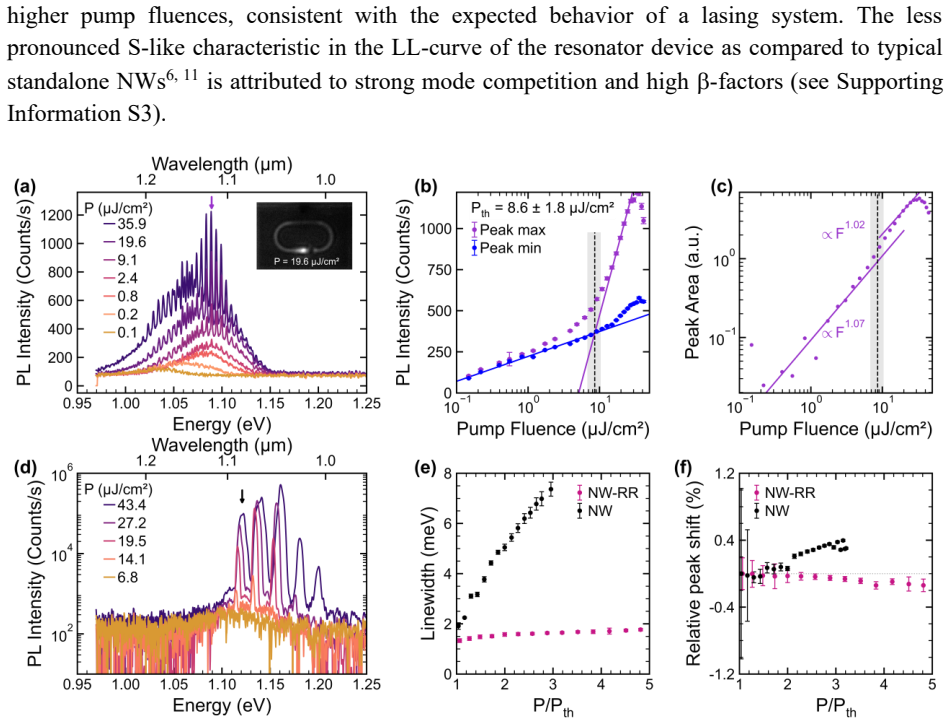
Transfer-printing GaAsSb NWs onto SOI racetrack resonators realizes optical feedback that induces lasing emission at a threshold of 8.6 ± 1.8 μJ/cm². The linewidth narrows by more than a factor of four at 3P_th and remains below 1.8 meV up to 5P_th, while FDTD simulations show efficient coupling between the hybrid NW-waveguide mode and the fundamental TE resonator mode with Q-factors exceeding 10^4. Control devices without the resonator exhibit broader and less stable emission.
What carries the argument
The SOI racetrack resonator coupled to the GaAsSb nanowire, which supplies resonator-driven optical feedback through the hybrid mode.
If this is right
- Lasing occurs at low pump fluence of 8.6 ± 1.8 μJ/cm².
- Linewidth drops by more than four times at three times threshold power.
- Linewidth stays below 1.8 meV up to five times threshold power.
- The approach functions at silicon-transparent wavelengths suitable for photonic integrated circuits.
Where Pith is reading between the lines
- The same transfer-printing method could be applied to other nanowire materials to reach additional wavelength bands.
- Adjusting resonator dimensions might increase feedback strength and further reduce threshold or linewidth.
- Integrated nanowire sources of this type could decrease the need for separate external cavities in compact photonic systems.
Load-bearing premise
That the observed linewidth narrowing and emission stability result specifically from optical feedback supplied by the SOI resonator rather than from differences in nanowire material quality or pumping conditions.
What would settle it
Measuring the same narrow linewidth and stability in control nanowires fabricated and pumped identically but without any SOI resonator would falsify the claim that feedback from the resonator is the cause.
Figures


read the original abstract
Silicon photonic integrated circuits critically depend on compact on-chip light sources, for which nanowire (NW) lasers are an attractive solution. However, their practical implementation is often limited by broad emission linewidths and poor frequency stability resulting from weak optical feedback. Here, we integrate individual GaAsSb NWs by transfer-printing onto silicon-on-insulator (SOI) racetrack resonators to realize optical feedback at silicon-transparent wavelengths. Finite-difference-time-domain simulations reveal efficient coupling between the hybrid NW-waveguide mode and the fundamental TE resonator mode, with calculated cavity Q-factors exceeding 10$^4$. Experimentally, we observe feedback-induced lasing emission at a low threshold (P$_{th}$) of 8.6 $\pm$ 1.8 $\mu$J/cm$^2$. Compared to identical NW lasers without SOI resonator, the linewidth is reduced by more than a factor of four at 3P$_{th}$ and remains stable below 1.8 meV up to 5P$_{th}$. Our results demonstrate NW-based light sources on SOI and show that tailored resonator designs enable improved linewidth control and frequency stabilization.
Editorial analysis
A structured set of objections, weighed in public.
Referee Report
Summary. The manuscript reports integration of GaAsSb nanowires onto SOI racetrack resonators via transfer-printing to provide optical feedback, supported by FDTD simulations showing Q-factors >10^4. Experiments claim feedback-induced lasing at threshold 8.6 ± 1.8 μJ/cm², with linewidth reduced by more than 4× at 3P_th and stable below 1.8 meV up to 5P_th relative to control NW lasers fabricated without the resonator.
Significance. If the linewidth narrowing and stability are confirmed to arise specifically from resonator feedback rather than fabrication artifacts, the work would advance compact on-chip sources for silicon photonics by demonstrating a practical route to improved frequency control in nanowire lasers.
major comments (2)
- [Results (experimental comparison)] The attribution of >4× linewidth reduction and stability below 1.8 meV (up to 5P_th) to resonator feedback rests on the direct comparison to 'identical NW lasers without SOI resonator'. Transfer-printing onto the racetrack may introduce local strain, surface modification, or alignment differences absent in controls, providing an alternative explanation independent of the calculated coupling. Additional characterization (e.g., Raman strain maps or defect density) of both sample sets is required to isolate the feedback mechanism.
- [Methods and Results] The quantitative threshold (8.6 ± 1.8 μJ/cm²) and linewidth stability claims cannot be fully verified without raw spectra, explicit data exclusion criteria, and confirmation that pumping conditions and NW material quality were matched between resonator and control devices. This absence raises the possibility of post-hoc selection effects in the reported stability.
minor comments (2)
- [Abstract] The abstract states silicon-transparent wavelengths but does not specify the operating range; adding this would clarify compatibility with SOI photonics.
- [Figures] Figure captions and legends should explicitly label error bars on threshold and linewidth data and indicate the number of devices measured for each condition.
Simulated Author's Rebuttal
We thank the referee for the constructive comments and the opportunity to clarify aspects of our work. We address each major comment point by point below, providing the strongest honest defense of the manuscript while acknowledging where revisions are warranted.
read point-by-point responses
-
Referee: [Results (experimental comparison)] The attribution of >4× linewidth reduction and stability below 1.8 meV (up to 5P_th) to resonator feedback rests on the direct comparison to 'identical NW lasers without SOI resonator'. Transfer-printing onto the racetrack may introduce local strain, surface modification, or alignment differences absent in controls, providing an alternative explanation independent of the calculated coupling. Additional characterization (e.g., Raman strain maps or defect density) of both sample sets is required to isolate the feedback mechanism.
Authors: The control NW lasers were fabricated from the same growth batch and subjected to the identical transfer-printing process, with the sole distinction being their placement on the SOI chip away from any resonator structures. This design ensures that transfer-induced strain, surface effects, and alignment variations are common to both sets. The observed >4× linewidth reduction and stability below 1.8 meV correlate directly with the presence of the racetrack and match the FDTD-predicted coupling efficiency and Q-factors >10^4. While Raman strain mapping was not performed, we have added a discussion in the revised manuscript citing literature values for transfer-printing strain in similar NW-SOI systems and explaining why such strain levels cannot account for the magnitude of the linewidth narrowing or its power dependence. The resonator-specific feedback remains the most consistent explanation. revision: partial
-
Referee: [Methods and Results] The quantitative threshold (8.6 ± 1.8 μJ/cm²) and linewidth stability claims cannot be fully verified without raw spectra, explicit data exclusion criteria, and confirmation that pumping conditions and NW material quality were matched between resonator and control devices. This absence raises the possibility of post-hoc selection effects in the reported stability.
Authors: We agree that greater transparency on data handling strengthens the claims. In the revised manuscript and supplementary information, we now include representative raw spectra from both resonator-integrated and control devices. We have added explicit text stating that all NWs exhibiting lasing were included in the statistics with no post-hoc exclusion based on linewidth or stability performance. Pumping conditions (wavelength, fluence, spot size, and repetition rate) were identical for all measurements, and NWs for both sample types were drawn from the same growth run to ensure matched material quality. These additions eliminate ambiguity regarding selection effects. revision: yes
Circularity Check
No circularity: experimental measurements and standard FDTD simulations are self-contained
full rationale
The paper reports experimental transfer-printing of GaAsSb NWs onto SOI racetrack resonators, FDTD simulations showing coupling and Q>10^4, and direct comparisons of lasing threshold (8.6 μJ/cm²) and linewidth narrowing (>4x at 3P_th, stable <1.8 meV to 5P_th) versus control NWs without resonators. No derivation chain, fitted parameter, or self-referential equation exists; claims rest on measured data and standard simulations without reducing to inputs by construction. Self-contained against external benchmarks.
Axiom & Free-Parameter Ledger
axioms (1)
- domain assumption Finite-difference time-domain simulations accurately predict coupling efficiency and Q-factors between the hybrid NW-waveguide mode and the fundamental TE resonator mode.
Reference graph
Works this paper leans on
-
[1]
Characterization, Selection, and Microassembly of Nanowire Laser Systems,
D. Jevtics et al., “Characterization, Selection, and Microassembly of Nanowire Laser Systems,” Nano Letters, vol. 20, no. 3, pp. 1862–1868, 2020, doi: 10.1021/acs.nanolett.9b05078
-
[2]
How Do the Purcell Factor, the Q‐Factor, and the Beta Factor Affect the Laser Threshold?,
J. B. Khurgin and M. A. Noginov, “How Do the Purcell Factor, the Q‐Factor, and the Beta Factor Affect the Laser Threshold?,” Laser & Photonics Reviews , vol. 15, no. 3, 2021, doi: 10.1002/lpor.202000250
discussion (0)
Sign in with ORCID, Apple, or X to comment. Anyone can read and Pith papers without signing in.