Sharp periodic Ge concentration modulations beyond the conduction band valley wavevector k₀ in nuclear spin-free Si quantum wells
Pith reviewed 2026-06-28 19:52 UTC · model grok-4.3
The pith
Periodic Ge modulations down to 0.49 nm periods are achieved in Si quantum wells, with simulations indicating valley splitting gains in 2k0/3 structures.
A machine-rendered reading of the paper's core claim, the machinery that carries it, and where it could break.
Core claim
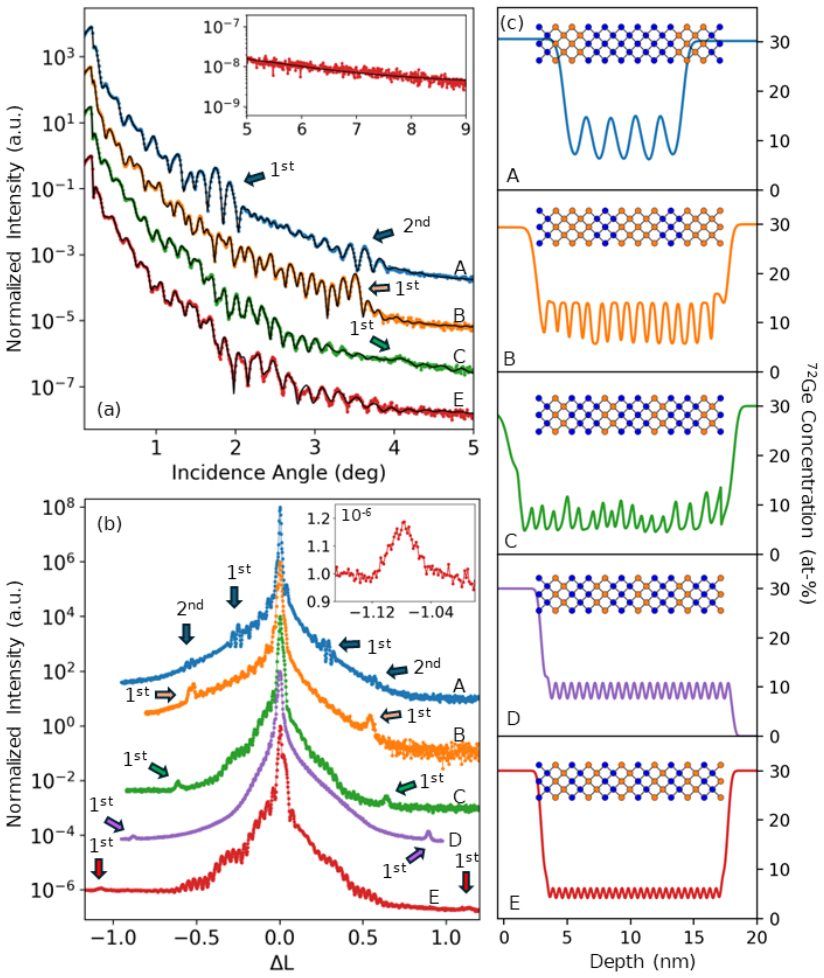
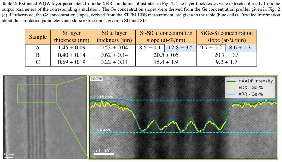
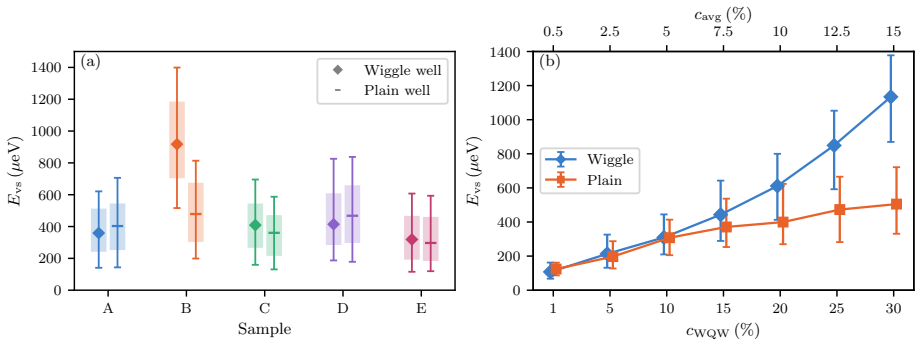
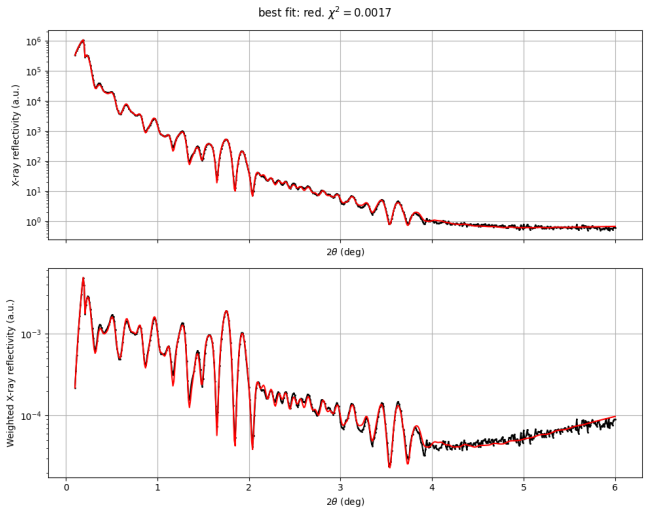
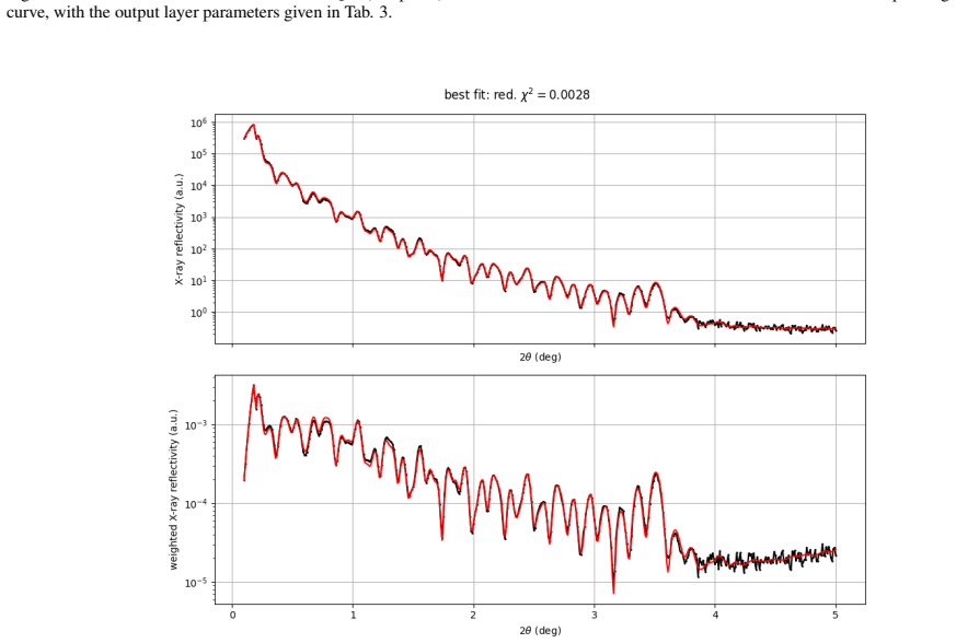
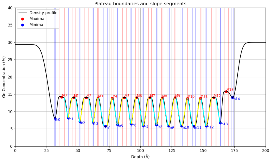
We demonstrate Ge-modulated Si quantum wells with periods from 2.00 to 0.49 nm, including modulations at k0 and 2k0/3. Synchrotron X-ray techniques and scanning transmission electron microscopy reveal laterally homogeneous Ge modulations over micrometer scales, with amplitudes up to 10 at-% and gradients reaching 20 at-%/nm. Two-bands k·p simulations suggest deterministic enhancement of valley splittings in steep trapezoidal 2k0/3 heterostructures, while the effect in k0-type quantum wells is much weaker.
What carries the argument
Periodic Ge concentration modulations with periods at or beyond the Si valley wavevector k0 (9.7 nm^{-1}), verified by X-ray and STEM imaging and evaluated for valley splitting via two-band k·p simulations.
If this is right
- Steep trapezoidal 2k0/3 Ge modulations produce deterministic valley splitting enhancement according to the simulations.
- k0-period wells yield much weaker splitting enhancement under the same modeling.
- The achieved modulations maintain lateral homogeneity over micrometer scales with up to 10 at-% amplitude and 20 at-%/nm gradients.
- These structures are grown using nuclear-spin-free 28Si and 72Ge sources.
Where Pith is reading between the lines
- Device-level tests would be needed to determine whether the ideal trapezoidal profiles survive processing and gating without extra scattering that reduces the predicted splitting.
- The demonstrated growth control over sub-nanometer periods could be applied to other modulation shapes or layer sequences to further tune valley or other band parameters.
- Homogeneous micrometer-scale modulation raises the possibility of placing many such quantum wells or dots on the same wafer with consistent properties.
Load-bearing premise
The fabricated Ge modulations will produce the valley splitting enhancement predicted by the two-band k·p simulations once placed inside actual gated quantum devices.
What would settle it
Fabricate and measure valley splitting in gated quantum dots from the 2k0/3 modulated wells and check whether the measured splitting matches the magnitude and dependence predicted by the k·p simulations for the reported trapezoidal profiles.
Figures


read the original abstract
Periodic Ge modulations within strained Si quantum wells in SiGe heterostructures offer a route to deterministically enhance conduction-band valley splitting in Si, a key requirement for scalable spin-qubit quantum computing. Efficient enhancement requires modulations in the order of the Si valley wavevector $k_0$ (9.7 nm$^{-1}$), corresponding to a period of 0.64 nm and near-monolayer growth control. Using nuclear-spin-free molecular beam epitaxy with $^{28}$Si and $^{72}$Ge, we demonstrate Ge-modulated Si quantum wells with periods from 2.00 to 0.49 nm, including modulations at $k_0$ and $2k_0/3$. Synchrotron X-ray techniques and scanning transmission electron microscopy reveal laterally homogeneous Ge modulations over micrometer scales, with amplitudes up to 10 at-% and gradients reaching 20 at-%/nm. Two-bands $\mathbf{k}\cdot\mathbf{p}$ simulations suggest deterministic enhancement of valley splittings in steep trapezoidal $2k_0/3$ heterostructures, while the effect in $k_0$-type quantum wells is much weaker.
Editorial analysis
A structured set of objections, weighed in public.
Referee Report
Summary. The manuscript reports epitaxial growth via nuclear-spin-free MBE of Si quantum wells containing periodic Ge modulations with periods from 2.00 nm down to 0.49 nm (including at k0 ≈ 0.64 nm and 2k0/3). Synchrotron X-ray diffraction and STEM imaging establish lateral homogeneity over micrometer scales, Ge amplitudes reaching 10 at-%, and concentration gradients up to 20 at-%/nm. Two-band k·p simulations are presented to indicate that steep trapezoidal 2k0/3 profiles can produce deterministic enhancement of conduction-band valley splitting, whereas the effect is weaker for k0-type wells.
Significance. If the simulated valley-splitting enhancement is realized in working devices, the approach would supply a growth-based route to deterministically lift valley degeneracy in Si, directly addressing a central obstacle to scalable spin-qubit architectures. The experimental achievement of sub-nanometer-period, laterally homogeneous Ge modulations with steep gradients constitutes a notable advance in SiGe heterostructure precision.
major comments (1)
- [Abstract] Abstract (final sentence): the deterministic-enhancement claim rests on two-band k·p simulations that assume ideal trapezoidal Ge profiles. The X-ray and STEM data confirm micrometer-scale homogeneity and gradients but supply no direct constraint on atomic-scale intermixing, interface roughness, or deviations from the assumed trapezoidal shape at the 0.49–0.65 nm periods; such deviations would alter the effective potential experienced by the valley states and could reduce or eliminate the predicted splitting enhancement.
Simulated Author's Rebuttal
We thank the referee for the careful review and positive evaluation of the experimental results. We address the single major comment below and agree that revisions are warranted to clarify the scope of the simulation-based claims.
read point-by-point responses
-
Referee: [Abstract] Abstract (final sentence): the deterministic-enhancement claim rests on two-band k·p simulations that assume ideal trapezoidal Ge profiles. The X-ray and STEM data confirm micrometer-scale homogeneity and gradients but supply no direct constraint on atomic-scale intermixing, interface roughness, or deviations from the assumed trapezoidal shape at the 0.49–0.65 nm periods; such deviations would alter the effective potential experienced by the valley states and could reduce or eliminate the predicted splitting enhancement.
Authors: We agree that the synchrotron X-ray and STEM data establish micrometer-scale lateral homogeneity and gradients up to 20 at-%/nm but cannot resolve atomic-scale intermixing, roughness, or exact deviations from the idealized trapezoidal Ge profiles at the 0.49–0.65 nm periods. The valley-splitting predictions therefore rely on the assumptions of the two-band k·p model. We will revise the abstract to explicitly qualify the enhancement statement by noting these assumptions and that experimental confirmation of the splitting remains for future device measurements. We will also add a brief discussion of the sensitivity of the splitting to profile imperfections. revision: yes
Circularity Check
No significant circularity; experimental characterization and standard k·p simulations remain independent of each other.
full rationale
The paper's core claims rest on direct MBE growth, synchrotron X-ray diffraction, and STEM imaging that measure periods, amplitudes, and gradients without reference to the valley-splitting predictions. The two-band k·p simulations are performed on idealized trapezoidal profiles using established theory and are presented only as suggestive; they are not fitted to the measured data nor used to retroactively define the reported structures. No self-citation chains, self-definitional loops, or fitted-input-as-prediction patterns appear in the provided text. The noted gap between ideal simulation profiles and possible atomic-scale deviations is a limitation of applicability, not a circularity in the derivation.
Axiom & Free-Parameter Ledger
axioms (1)
- domain assumption Two-band k·p theory accurately models valley splitting in the described SiGe heterostructures
Reference graph
Works this paper leans on
-
[1]
Semiconductor spin qubits,
G. Burkard, T. D. Ladd, A. Pan, J. M. Nichol, and J. R. Petta, “Semiconductor spin qubits,”Rev. Mod. Phys., vol. 95, p. 025003, Jun 2023
2023
-
[2]
Nanoscale ‘conveyor belt’ teleports quantum state of electron,
L. R. Schreiber, “Nanoscale ‘conveyor belt’ teleports quantum state of electron,”Nature, vol. 650, pp. 14–15, 2026
2026
-
[3]
Universal control of a six- qubit quantum processor in silicon,
S. G. J. Philips, M. T. Madzik, S. V . Amitonov, S. L. de Snoo, M. Russ, N. Kalhor, C. V olk, W. I. L. Lawrie, D. Brousse, L. Tryputen, B. P. Wuetz, A. Sammak, M. Veldhorst, G. Scap- pucci, and L. M. K. Vandersypen, “Universal control of a six- qubit quantum processor in silicon,”Nature, vol. 609, pp. 919– 924, Sep 2022
2022
-
[4]
Running a six-qubit quantum circuit on a silicon spin qubit array,
I. F. de Fuentes, E. Raymenants, B. Undseth, O. Pietx-Casas, S. P. M. M˛ adzik, S. L. de Snoo, S. V . Amitonov, L. Tryputen, A. T. Schmitz, A. Y . Matsuura, G. Scappucci, and L. M. K. Van- dersypen, “Running a six-qubit quantum circuit on a silicon spin qubit array,”arXiv preprint 2505.19200, 2025
-
[5]
A digitally controlled silicon quantum processing unit
Members of HRL Quantum Team and Collaborators, “A digi- tally controlled silicon quantum processing unit,”arXiv preprint 2604.16216, 2026
work page internal anchor Pith review Pith/arXiv arXiv 2026
-
[6]
Fast universal quantum gate above the fault-tolerance threshold in silicon,
A. Noiri, K. Takeda, T. Nakajima, T. Kobayashi, A. Sammak, G. Scappucci, and S. Tarucha, “Fast universal quantum gate above the fault-tolerance threshold in silicon,”Nature, vol. 601, p. 338, Jan. 2022
2022
-
[7]
Two-qubit silicon quan- tum processor with operation fidelity exceeding 99%,
A. R. Mills, C. R. Guinn, M. J. Gullans, A. J. Sigillito, M. M. Feldman, E. Nielsen, and J. R. Petta, “Two-qubit silicon quan- tum processor with operation fidelity exceeding 99%,”Sci. Adv., vol. 8, p. 5130, 2022
2022
-
[8]
Quantum logic with spin qubits crossing the surface code threshold,
X. Xue, M. Russ, N. Samkharadze, B. Undseth, A. Sammak, G. Scappucci, and L. M. K. Vandersypen, “Quantum logic with spin qubits crossing the surface code threshold,”Nature, vol. 601, no. 7893, p. 343, 2022
2022
-
[9]
Simultaneous high-fidelity single-qubit gates in a spin qubit array,
Y .-H. Wu, L. C. Camenzind, P. Bütler, I. K. Jin, A. Noiri, K. Takeda, T. Nakajima, T. Kobayashi, G. Scappucci, H.-S. Goan, and S. Tarucha, “Simultaneous high-fidelity single-qubit gates in a spin qubit array,”arXiv preprint 2507.11918, 2025
-
[10]
Low-frequency spin qubit energy splitting noise in highly purified 28Si/SiGe,
T. Struck, A. Hollmann, F. Schauer, O. Fedorets, A. Schmid- bauer, K. Sawano, H. Riemann, N. V . Abrosimov, L. Cywinski, D. Bougeard, and L. R. Schreiber, “Low-frequency spin qubit energy splitting noise in highly purified 28Si/SiGe,”npj Quan- tum Inf., vol. 6, no. 69, p. 2056, 2020
2056
-
[11]
Review of performance metrics of spin qubits in gated semiconducting nanostructures,
P. Stano and D. Loss, “Review of performance metrics of spin qubits in gated semiconducting nanostructures,”Nat. Rev. Phys., vol. 4, p. 672, Oct. 2022
2022
-
[12]
Coherence limit due to hyperfine interaction with nuclei in the barrier material of si spin qubits,
L. Cvitkovich, P. Stano, C. Wilhelmer, D. Waldhör, D. Loss, Y .- M. Niquet, and T. Grasser, “Coherence limit due to hyperfine interaction with nuclei in the barrier material of si spin qubits,” Physical Review Applied, vol. 22, no. 6, p. 064089, 2024
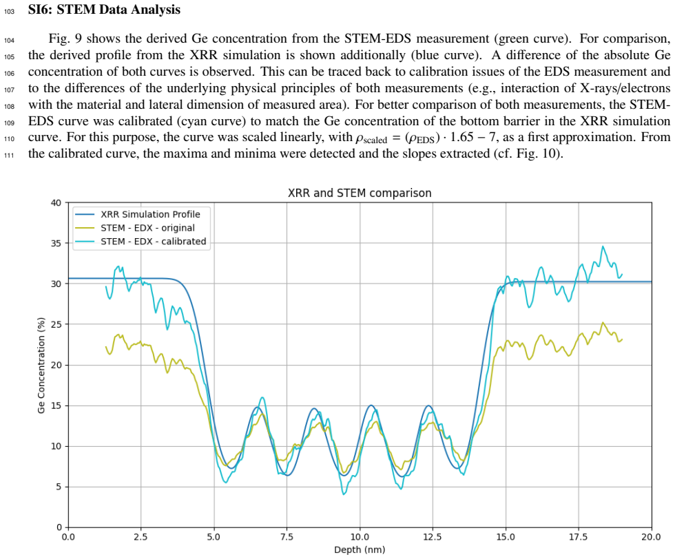
2024
-
[13]
High-fidelity single-spin shuttling in silicon,
M. De Smet, Y . Matsumoto, A.-M. J. Zwerver, L. Tryputen, S. L. de Snoo, S. V . Amitonov, S. R. Katiraee-Far, A. Sammak, N. Samkharadze, O. Guel, R. N. M. Wasserman, E. Greplová, M. Rimbach-Russ, G. Scappucci, and L. M. K. Vandersypen, “High-fidelity single-spin shuttling in silicon,”Nat. Nanotech- nol., vol. 20, pp. 866–872, July 2025
2025
-
[14]
Si/SiGe qubus for single electron information-processing devices with memory and micron-scale connectivity function,
R. Xue, M. Beer, I. Seidler, S. S. Humpohl, J.-S. Tu, S. Trel- lenkamp, T. Struck, H. Bluhm, and L. R. Schreiber, “Si/SiGe qubus for single electron information-processing devices with memory and micron-scale connectivity function,”Nature Com- munications, vol. 15, p. 2296, 2024
2024
-
[15]
Conveyor-mode electron shuttling through a t-junction in si/sige,
M. Beer, R. Xue, L. Deda, S. Trellenkamp, J.-S. Tu, P. Sur- rey, I. Seidler, H. Bluhm, and L. R. Schreiber, “Conveyor-mode electron shuttling through a t-junction in si/sige,”arXiv preprint 2601.03942, 2026
-
[16]
Two-qubit logic and teleportation with mobile spin qubits in silicon,
Y . Matsumoto, M. D. Smet, L. Tryputen, S. L. de Snoo, S. V . Amitonov, A. Sammak, M. Rimbach-Russ, G. Scappucci, and L. M. K. Vandersypen, “Two-qubit logic and teleportation with mobile spin qubits in silicon,”Nature, vol. 650, pp. 56–61, 2026
2026
-
[17]
Spiderweb array: A sparse spin- qubit array,
J. M. Boter, J. P. Dehollain, J. P. van Dijk, Y . Xu, T. Hensgens, R. Versluis, H. W. Naus, J. S. Clarke, M. Veldhorst, F. Sebas- tiano, and L. M. Vandersypen, “Spiderweb array: A sparse spin- qubit array,”Phys. Rev. Appl., vol. 18, p. 024053, Aug 2022
2022
-
[18]
The spinbus architecture for scaling spin qubits with electron shuttling,
M. Künne, A. Willmes, M. Oberländer, C. Gorjaew, J. D. Teske, H. Bhardwaj, M. Beer, E. Kammerloher, R. Otten, I. Seidler, et al., “The spinbus architecture for scaling spin qubits with electron shuttling,”Nature Communications, vol. 15, no. 1, p. 4977, 2024
2024
-
[19]
12-Spin-Qubit Arrays Fabricated on a 300 mm Semiconductor Manufacturing Line,
H. C. George, M. T. M˛ adzik, E. M. Henry, A. J. Wagner, M. M. Islam, F. Borjans, E. J. Connors, J. Corrigan, M. Curry, M. K. Harper, D. Keith, L. Lampert, F. Luthi, F. A. Mohiyaddin, S. Murcia, R. Nair, R. Nahm, A. Nethwewala, S. Neyens, B. Pa- tra, R. D. Raharjo, C. Rogan, R. Savytskyy, T. F. Watson, J. Ziegler, O. K. Zietz, S. Pellerano, R. Pillarisett...
2025
-
[20]
High-fidelity single-electron shuttling in industrially fabricated spin qubit devices,
P. Muster, W. Langheinrich, T. Huckemann, S. Pregl, V . Brack- mann, M. Friedrich, F. Reichmann, N. D. Komeri ˇcki, L. R. Schreiber, and J. Bluhm, “High-fidelity single-electron shuttling in industrially fabricated spin qubit devices,” in2025 IEEE In- ternational Electron Devices Meeting (IEDM), pp. 1–4, IEEE, 2025
2025
-
[21]
Valley splitting in Si/SiGe het- erostructures from first principles,
L. Cvitkovich, T. Salamone, C. Wilhelmer, B. Martinez, T. Grasser, and Y .-M. Niquet, “Valley splitting in Si/SiGe het- erostructures from first principles,”Physical Review B, vol. 113, no. 3, p. 035307, 2026
2026
-
[22]
Valley splitting correlations across a silicon quantum well con- taining germanium,
J. C. Marcks, E. Eagen, E. C. Brann, M. P. Losert, T. Oh, J. Reily, C. S. Wang, D. Keith, F. A. Mohiyaddin, F. Luthi,et al., “Valley splitting correlations across a silicon quantum well con- taining germanium,”Nature Communications, vol. 16, no. 1, p. 11381, 2025
2025
-
[23]
Valley splitting depending on the size and location of a silicon quantum dot,
J. R. Lima and G. Burkard, “Valley splitting depending on the size and location of a silicon quantum dot,”Physical Review Materials, vol. 8, no. 3, p. 036202, 2024
2024
-
[24]
Mapping of valley splitting by conveyor-mode spin-coherent electron shuttling,
M. V olmer, T. Struck, A. Sala, B. Chen, M. Oberländer, T. Offer- mann, R. Xue, L. Visser, J.-S. Tu, S. Trellenkamp, L. Cywinski, H. Bluhm, and L. R. Schreiber, “Mapping of valley splitting by conveyor-mode spin-coherent electron shuttling,”npj Quantum Inf., vol. 10, p. 61, June 2024
2024
-
[25]
Impact of valley phase and split- ting on readout of silicon spin qubits,
M. L. V . Tagliaferri, P. L. Bavdaz, W. Huang, A. S. Dzurak, D. Culcer, and M. Veldhorst, “Impact of valley phase and split- ting on readout of silicon spin qubits,”Phys. Rev. B, vol. 97, p. 245412, June 2018
2018
-
[26]
Large, tunable valley splitting and single-spin relaxation mechanisms in a Si/SixGe1−x quantum dot,
A. Hollmann, T. Struck, V . Langrock, A. Schmidbauer, F. Schauer, T. Leonhardt, K. Sawano, H. Riemann, N. V . Abrosi- mov, D. Bougeard, and L. R. Schreiber, “Large, tunable valley splitting and single-spin relaxation mechanisms in a Si/SixGe1−x quantum dot,”Phys. Rev. Appl., vol. 13, p. 034068, Mar. 2020
2020
-
[27]
Blueprint of a scalable spin qubit shuttle device for coherent mid-range qubit transfer in disor- dered Si/SiGe/SiO 2,
V . Langrock, J. A. Krzywda, N. Focke, I. Seidler, L. R. Schreiber, and Ł. Cywi ´nski, “Blueprint of a scalable spin qubit shuttle device for coherent mid-range qubit transfer in disor- dered Si/SiGe/SiO 2,”PRX Quantum, vol. 4, p. 020305, Apr. 2023
2023
-
[28]
M. V olmer, T. Struck, J.-S. Tu, S. Trellenkamp, D. D. Es- posti, G. Scappucci, Łukasz Cywi ´nski, H. Bluhm, and L. R. Schreiber, “Impact of the local valley splitting on the coherence of conveyor-belt spin shuttling in 28Si/SiGe,”arXiv preprint 2510.03773, 2026
work page internal anchor Pith review Pith/arXiv arXiv 2026
-
[29]
Strate- 10 gies for enhancing spin-shuttling fidelities in Si/SiGe quan- tum wells with random-alloy disorder,
M. P. Losert, M. Oberländer, J. D. Teske, M. V olmer, L. R. Schreiber, H. Bluhm, S. Coppersmith, and M. Friesen, “Strate- 10 gies for enhancing spin-shuttling fidelities in Si/SiGe quan- tum wells with random-alloy disorder,”PRX Quantum, vol. 5, p. 040322, Nov. 2024
2024
-
[30]
Long distance spin shuttling en- abled by few-parameter velocity optimization,
A. David, A. M. Pazhedath, L. R. Schreiber, T. Calarco, H. Bluhm, and F. Motzoi, “Long distance spin shuttling en- abled by few-parameter velocity optimization,”arXiv preprint arXiv:2409.07600, 2024
-
[31]
Practical strategies for en- hancing the valley splitting in si/sige quantum wells,
M. P. Losert, M. Eriksson, R. Joynt, R. Rahman, G. Scappucci, S. N. Coppersmith, and M. Friesen, “Practical strategies for en- hancing the valley splitting in si/sige quantum wells,”Physical Review B, vol. 108, no. 12, p. 125405, 2023
2023
-
[32]
Engineering ge profiles in Si/SiGe heterostruc- tures for increased valley splitting,
L. E. Stehouwer, M. P. Losert, M. Rigot, D. Degli Esposti, S. Martí-Sánchez, M. Rimbach-Russ, J. Arbiol, M. Friesen, and G. Scappucci, “Engineering ge profiles in Si/SiGe heterostruc- tures for increased valley splitting,”Nano Letters, vol. 25, no. 34, pp. 12892–12898, 2025
2025
-
[33]
Valley splittings in Si/SiGe quantum dots with a germanium spike in the silicon well,
T. McJunkin, E. R. MacQuarrie, L. Tom, S. F. Neyens, J. P. Dod- son, B. Thorgrimsson, J. Corrigan, H. E. Ercan, D. E. Savage, M. G. Lagally, R. Joynt, S. N. Coppersmith, M. Friesen, and M. A. Eriksson, “Valley splittings in Si/SiGe quantum dots with a germanium spike in the silicon well,”Phys. Rev. B, vol. 104, p. 085406, Aug. 2021
2021
-
[34]
Atomic fluctuations lifting the energy degeneracy in Si/SiGe quantum dots,
B. Paquelet Wuetz, M. P. Losert, S. Koelling, L. E. A. Ste- houwer, A.-M. J. Zwerver, S. G. J. Philips, M. T. Ma ¸dzik, X. Xue, G. Zheng, M. Lodari, S. V . Amitonov, N. Samkharadze, A. Sammak, L. M. K. Vandersypen, R. Rahman, S. N. Copper- smith, O. Moutanabbir, M. Friesen, and G. Scappucci, “Atomic fluctuations lifting the energy degeneracy in Si/SiGe qu...
2022
-
[35]
Atom- istic compositional details and their importance for spin qubits in isotope-purified silicon quantum wells,
J. Klos, J. Tröger, J. Keutgen, M. P. Losert, N. V . Abrosi- mov, J. Knoch, H. Bracht, S. N. Coppersmith, M. Friesen, O. Cojocaru-Mirédin, L. R. Schreiber, and D. Bougeard, “Atom- istic compositional details and their importance for spin qubits in isotope-purified silicon quantum wells,”Adv. Sci., vol. 11, p. 2407442, Nov. 2024
2024
-
[36]
SiGe quan- tum wells with oscillating Ge concentrations for quantum dot qubits,
T. McJunkin, B. Harpt, Y . Feng, M. P. Losert, R. Rahman, J. P. Dodson, M. A. Wolfe, D. E. Savage, M. G. Lagally, S. N. Cop- persmith, M. Friesen, R. Joynt, and M. A. Eriksson, “SiGe quan- tum wells with oscillating Ge concentrations for quantum dot qubits,”Nature Communications, vol. 13, p. 7777, Dec. 2022
2022
-
[37]
Enhanced valley splitting in si layers with oscillatory ge concentration,
Y . Feng and R. Joynt, “Enhanced valley splitting in si layers with oscillatory ge concentration,”Physical Review B, vol. 106, no. 8, p. 085304, 2022
2022
-
[38]
Theory of valley split- ting in Si/SiGe spin qubits: Interplay of strain, resonances, and random alloy disorder,
A. Thayil, L. Ermoneit, and M. Kantner, “Theory of valley split- ting in Si/SiGe spin qubits: Interplay of strain, resonances, and random alloy disorder,”Physical Review B, vol. 112, no. 11, p. 115303, 2025
2025
-
[39]
Spin- orbit enhancement in si/sige heterostructures with oscillating ge concentration,
B. D. Woods, M. Eriksson, R. Joynt, and M. Friesen, “Spin- orbit enhancement in si/sige heterostructures with oscillating ge concentration,”Physical Review B, vol. 107, no. 3, p. 035418, 2023
2023
-
[40]
Enhanced nanoscale Ge concentration os- cillations in Si/SiGe quantum well through controlled segrega- tion,
K.-P. Gradwohl, L. Cvitkovich, C.-H. Lu, S. Koelling, M. Oezkent, Y . Liu, D. Waldhör, T. Grasser, Y .-M. Niquet, M. Albrecht,et al., “Enhanced nanoscale Ge concentration os- cillations in Si/SiGe quantum well through controlled segrega- tion,”Nano Letters, vol. 25, no. 11, pp. 4204–4210, 2025
2025
-
[41]
Coupling conduction-band val- leys in SiGe heterostructures via shear strain and Ge concen- tration oscillations,
B. D. Woods, H. Soomro, E. Joseph, C. C. Frink, R. Joynt, M. Eriksson, and M. Friesen, “Coupling conduction-band val- leys in SiGe heterostructures via shear strain and Ge concen- tration oscillations,”npj Quantum Information, vol. 10, no. 1, p. 54, 2024
2024
-
[42]
Increasing valley splitting in Si/SiGe by practically achievable heterostructure profiles,
L. Cvitkovich, P. Stano, D. Bougeard, Y .-M. Niquet, and D. Loss, “Increasing valley splitting in Si/SiGe by practically achievable heterostructure profiles,”arXiv preprint 2603.19769, 2026
-
[43]
Epitaxy of strained, nuclear-spin free 76Ge quantum wells from solid source materials,
M. Oezkent, C.-H. Lu, L. Becker, S. Koelling, R. H. Blick, E. Rahier, S. Schönert, N. Abrosimov, T. Remmele, T. Boeck,et al., “Epitaxy of strained, nuclear-spin free 76Ge quantum wells from solid source materials,”arXiv preprint arXiv:2603.06372, 2026
-
[44]
Valley physics in the two-bandk·pmodel for sige heterostruc- tures and spin qubits,
T. Salamone, B. M. Diaz, J. Li, L. Cvitkovich, and Y .-M. Niquet, “Valley physics in the two-bandk·pmodel for sige heterostruc- tures and spin qubits,”Phys. Rev. B, vol. 113, p. 115304, Mar 2026
2026
-
[45]
Mapping g-factors and complex intervalley cou- pling in Si/SiGe by conveyor-mode shuttling,
M. V olmer, T. Struck, A. Sala, J.-S. Tu, S. Trellenkamp, D. D. Esposti, G. Scappucci, Łukasz Cywi ´nski, H. Bluhm, and L. R. Schreiber, “Mapping g-factors and complex intervalley cou- pling in Si/SiGe by conveyor-mode shuttling,”arXiv preprint 2603.01844, 2026
-
[46]
Onsite matrix elements of the tight-binding hamiltonian of a strained crystal: Application to silicon, germanium, and their alloys,
Y . M. Niquet, D. Rideau, C. Tavernier, H. Jaouen, and X. Blase, “Onsite matrix elements of the tight-binding hamiltonian of a strained crystal: Application to silicon, germanium, and their alloys,”Phys. Rev. B, vol. 79, p. 245201, Jun 2009. 11 Supplementary Information: Sharp periodic Ge concentration modulations beyond the conduction band valley wavevec...
2009
-
[47]
Parratt, L. G. Surface studies of solids by total reflection of x-rays.Phys. Rev.95, 359–369 (1954). URL219 https://link.aps.org/doi/10.1103/PhysRev.95.359.220
-
[48]
P.et al.Practical strategies for enhancing the valley splitting in si/SiGe quantum wells108, 125405
Losert, M. P.et al.Practical strategies for enhancing the valley splitting in si/SiGe quantum wells108, 125405. URL221 https://link.aps.org/doi/10.1103/PhysRevB.108.125405.222
-
[49]
Salamone, T., Diaz, B. M., Li, J., Cvitkovich, L. & Niquet, Y .-M. Valley physics in the two-bandk·pmodel for sige heterostructures and spin223 qubits.Phys. Rev. B113, 115304 (2026). URLhttps://link.aps.org/doi/10.1103/vhwf-qbnc.224
-
[50]
M., Rideau, D., Tavernier, C., Jaouen, H
Niquet, Y . M., Rideau, D., Tavernier, C., Jaouen, H. & Blase, X. Onsite matrix elements of the tight-binding hamiltonian of a strained crystal:225 Application to silicon, germanium, and their alloys.Phys. Rev. B79, 245201 (2009).226
2009
-
[51]
Feng, Y . & Joynt, R. Enhanced valley splitting in si layers with oscillatory ge concentration106, 085304. URL227 https://link.aps.org/doi/10.1103/PhysRevB.106.085304.228 21
discussion (0)
Sign in with ORCID, Apple, or X to comment. Anyone can read and Pith papers without signing in.