Modeling, Optimizing and Exploring Multi-Die FPGA Routing Architectures
Pith reviewed 2026-06-27 23:05 UTC · model grok-4.3
The pith
With suitable inter-die routing, 3D FPGAs cut wirelength up to 14% and critical path delay 6% versus 2D while staying routable.
A machine-rendered reading of the paper's core claim, the machinery that carries it, and where it could break.
Core claim
With suitable inter-die routing architectures, 2.5D and 3D FPGAs increase capacity without significant routability or delay penalties. Specifically, 3D FPGAs achieve up to 14% wirelength reduction and 6% CPD improvement over 2D devices and remain routable even with existing 10μm pitch technologies, while 2.5D FPGAs incur only a 2% wirelength and 4% CPD overhead at 32% inter-die connectivity.
What carries the argument
An extended VTR/VPR CAD flow augmented with HSPICE models of inter-die connections across 7 nm active dice and 45 nm interposers, plus modified placement and routing algorithms that optimize for multi-die topologies.
If this is right
- 3D FPGAs can deliver up to 14% shorter total wirelength and 6% better critical path delay than equivalent 2D devices.
- Multi-die FPGAs stay routable down to current 10 μm inter-die pitches when the routing architecture is chosen appropriately.
- 2.5D designs incur only 2% wirelength and 4% CPD penalty at 32% inter-die connectivity levels.
- Capacity scaling through die stacking is possible without forcing large increases in area or routing resources.
Where Pith is reading between the lines
- The same modeling approach could be applied to evaluate 3D stacking in other reconfigurable fabrics or even ASICs.
- Future process nodes with denser inter-die links would likely widen the performance advantage shown for 3D organizations.
- Open-sourcing the extensions allows direct comparison of multi-die FPGA designs against emerging monolithic 3D alternatives.
Load-bearing premise
The HSPICE circuit models of inter-die connections for a 7 nm process and 45 nm silicon interposer accurately predict the latency, density, and electrical behavior that will appear in real fabricated devices.
What would settle it
Build and measure a physical 3D FPGA prototype using one of the modeled inter-die routing schemes and compare its measured wirelength and critical path delay directly against the tool predictions.
Figures
read the original abstract
Die stacking has enabled 2.5D FPGAs by integrating multiple active dice on a passive silicon interposer for improved yield and capacity, and paved the way for 3D architectures that stack active dice directly atop one another. In these multi-die devices, the unique electrical and physical characteristics of the underlying die-stacking technology impose limitations on inter-die connection density and latency, necessitating a bespoke inter-die routing architecture. However, the absence of accurate and versatile modeling tools has left most questions about how to best design the inter-die routing architecture unanswered. To address this gap, we enhance the open-source FPGA CAD tool VTR to flexibly model a wide range of multi-die routing architectures, and augment VPR's placement and routing engines to improve optimization for both 2.5D and 3D FPGAs. We perform HSPICE-based circuit modeling of inter-die connections for active dice using a 7 nm process node and a 45 nm silicon interposer across several die-crossing technologies. Using this enhanced framework, we conduct a detailed design space exploration of inter-die routing architecture in 2.5D and 3D FPGAs, characterizing the impact of die-crossing technology, inter-die connection count, fan-in/fan-out, and interposer wire length on critical path delay (CPD), wirelength, area, and routability. Our results show that with suitable inter-die routing architectures, 2.5D and 3D FPGAs can increase capacity without significant routability or delay penalties. Specifically, 3D FPGAs achieve up to 14% wirelength reduction and 6% CPD improvement over 2D devices, and remain routable even with existing $10\,\mu$m pitch technologies, while 2.5D FPGAs incur only a 2% wirelength and 4% CPD overhead at 32% inter-die connectivity. All extensions are open source and integrated with the VTR master branch.
Editorial analysis
A structured set of objections, weighed in public.
Referee Report
Summary. The paper enhances the open-source VTR framework (including VPR placement/routing) to model and optimize inter-die routing architectures for 2.5D (silicon interposer) and 3D FPGAs. It performs HSPICE circuit modeling of inter-die connections using a 7 nm process node for active dice and 45 nm interposer across multiple die-crossing technologies, then uses the augmented CAD flow to explore the impact of connection density, fan-in/fan-out, and wire length on CPD, wirelength, area, and routability. The central claim is that suitable inter-die architectures allow capacity scaling with limited penalties: 3D FPGAs achieve up to 14% wirelength reduction and 6% CPD improvement versus 2D while remaining routable at 10 μm pitch; 2.5D FPGAs incur only 2% wirelength and 4% CPD overhead at 32% inter-die connectivity. All extensions are released open-source and merged into the VTR master branch.
Significance. If the HSPICE-derived electrical parameters prove representative of fabricated stacks, the work is significant as the first open-source, flexible CAD framework for systematic design-space exploration of multi-die FPGA routing. The explicit release and VTR integration, combined with the parameter sweeps over connection count and fan-in/fan-out, supply reproducible data and tooling that the community can use to evaluate 2.5D/3D trade-offs. This directly addresses the modeling gap noted in the abstract and supplies concrete quantitative guidance on routability at existing pitches.
major comments (2)
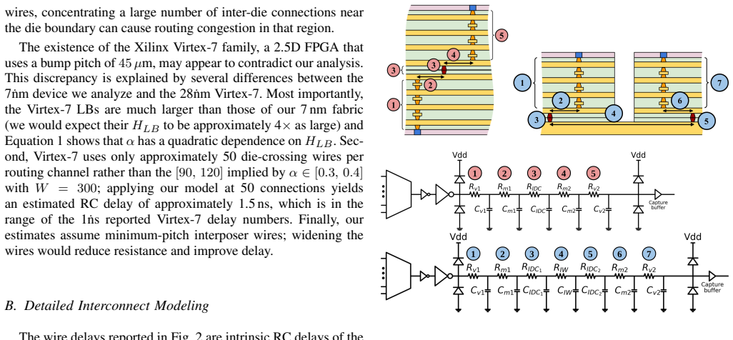
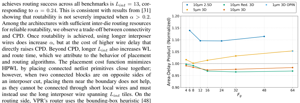
- [HSPICE modeling (Abstract + methods)] HSPICE modeling paragraph (Abstract) and associated methods: The manuscript describes the HSPICE setup for 7 nm dice + 45 nm interposer but reports no calibration against published TSV/micro-bump silicon measurements, no process-corner validation, and no sensitivity sweeps (e.g., ±20 % inter-die capacitance). Because every headline percentage (14 % WL reduction, 6 % CPD gain, 2 %/4 % 2.5D overhead, routability at 10 μm pitch) is produced by feeding the resulting RC/delay values into the modified VPR, the absence of validation is load-bearing for the central claim that “suitable inter-die routing architectures” incur “no significant routability or delay penalties.”
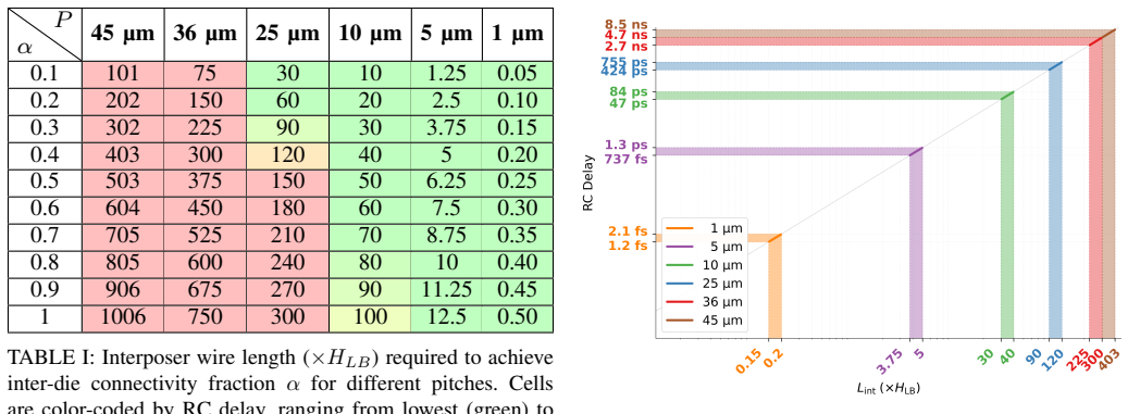
- [Results on 3D FPGAs] Results on 3D routability at 10 μm pitch: The statement that 3D devices “remain routable even with existing 10 μm pitch technologies” rests entirely on the unvalidated HSPICE delay model. A concrete sensitivity test showing how the reported routability margin changes under plausible model error would be required to support the claim.
minor comments (1)
- [Abstract] Abstract: the phrase “several die-crossing technologies” is used without enumerating them; an explicit list would improve readability.
Simulated Author's Rebuttal
We thank the referee for the detailed and constructive review. The comments on HSPICE modeling validation are well-taken and highlight an area where the manuscript can be strengthened. We address each major comment below.
read point-by-point responses
-
Referee: [HSPICE modeling (Abstract + methods)] HSPICE modeling paragraph (Abstract) and associated methods: The manuscript describes the HSPICE setup for 7 nm dice + 45 nm interposer but reports no calibration against published TSV/micro-bump silicon measurements, no process-corner validation, and no sensitivity sweeps (e.g., ±20 % inter-die capacitance). Because every headline percentage (14 % WL reduction, 6 % CPD gain, 2 %/4 % 2.5D overhead, routability at 10 μm pitch) is produced by feeding the resulting RC/delay values into the modified VPR, the absence of validation is load-bearing for the central claim that “suitable inter-die routing architectures” incur “no significant routability or delay penalties.”
Authors: We acknowledge that the manuscript does not include direct calibration of the HSPICE models against published silicon measurements for TSVs or micro-bumps, nor process-corner validation or sensitivity sweeps. The models rely on standard foundry PDKs for the specified nodes. In the revised manuscript we will add a dedicated sensitivity analysis section that varies inter-die capacitance and resistance by ±20 % (and other key RC parameters) and reports the resulting changes to CPD, wirelength, and routability margins. This will quantify the robustness of the headline claims under plausible model error while remaining within the scope of a CAD modeling study. revision: yes
-
Referee: [Results on 3D FPGAs] Results on 3D routability at 10 μm pitch: The statement that 3D devices “remain routable even with existing 10 μm pitch technologies” rests entirely on the unvalidated HSPICE delay model. A concrete sensitivity test showing how the reported routability margin changes under plausible model error would be required to support the claim.
Authors: We agree that the routability claim at 10 μm pitch would be more robust with an explicit sensitivity test. The sensitivity analysis described in our response to the first comment will directly address this by showing how the routability margin at 10 μm pitch varies under the same ±20 % parameter perturbations. The revised manuscript will include these results to support the statement that suitable architectures remain routable with existing pitches. revision: yes
Circularity Check
No circularity: results from independent HSPICE modeling fed into extended open-source VPR/VTR
full rationale
The paper performs HSPICE circuit modeling of inter-die connections using a 7 nm process and 45 nm interposer, then augments the existing VTR/VPR placement and routing engines to explore architecture parameters. All quantitative results (wirelength, CPD, routability) are produced by running the modified tool on standard benchmarks with the externally-simulated RC/delay values as inputs. No equations in the manuscript define a quantity in terms of itself, no fitted parameter is relabeled as a prediction, and no load-bearing claim reduces to a self-citation chain. The derivation chain is therefore self-contained against external simulation and benchmark data.
Axiom & Free-Parameter Ledger
axioms (1)
- domain assumption HSPICE circuit models for 7 nm active dice and 45 nm interposer accurately represent real inter-die electrical behavior and latency
Reference graph
Works this paper leans on
-
[1]
Field-programmable gate array ar- chitecture for deep learning: Survey and future directions,
A. Boutros, A. Arora, and V . Betz, “Field-programmable gate array ar- chitecture for deep learning: Survey and future directions,”Proceedings of the IEEE, 2025
2025
-
[2]
Accelerating RTL simulation with hardware-software co- design,
F. Elsabbagh, S. Sheikhha, V . A. Ying, Q. M. Nguyen, J. S. Emer, and D. Sanchez, “Accelerating RTL simulation with hardware-software co- design,” inProceedings of the 56th Annual IEEE/ACM International Symposium on Microarchitecture, 2023, pp. 153–166
2023
-
[3]
Makinote: An FPGA-based HW/SW platform for pre-silicon emulation of RISC-V designs,
E. Perdomo, A. Kropotov, F. K. Cano Ladino, S. Zafar, T. Cervero, X. M. Bofill, and B. Salami, “Makinote: An FPGA-based HW/SW platform for pre-silicon emulation of RISC-V designs,” inProceedings of the 16th Workshop on Rapid Simulation and Performance Evaluation for Design, 2024, pp. 29–34
2024
-
[4]
MangoBoost alice: Extremely fast, seamless, and versatile FPGA-accelerated DPU solutions,
H. Jeong, W. Lee, E. Baek, C. Kim, C. Jo, D. Chae, K. Choi, H. Jang, M. Elgammal, S. Honget al., “MangoBoost alice: Extremely fast, seamless, and versatile FPGA-accelerated DPU solutions,”IEEE Micro, vol. 45, no. 5, pp. 43–55, 2025
2025
-
[5]
Galapagos: A full stack approach to FPGA integration in the cloud,
N. Tarafdar, N. Eskandari, V . Sharma, C. Lo, and P. Chow, “Galapagos: A full stack approach to FPGA integration in the cloud,”IEEE Micro, vol. 38, no. 6, pp. 18–24, 2018
2018
-
[6]
A survey on FPGA-based heterogeneous clusters architectures,
W. F. Samayoa, M. L. Crespo, A. Cicuttin, and S. Carrato, “A survey on FPGA-based heterogeneous clusters architectures,”IEEE Access, vol. 11, pp. 67 679–67 706, 2023
2023
-
[7]
Cramming more components onto integrated circuits,
G. Moore, “Cramming more components onto integrated circuits,” Proceedings of the IEEE, vol. 86, no. 1, pp. 82–85, 1998
1998
-
[8]
TDM signal grouping and package pin assignment for 2.5 d multi-FPGA systems with lookahead placement,
J. Wang, R. Tao, J. Mai, X. Jiang, S. Wang, C. Yang, H. Jie, K. Huang, R. Y . Sun, and Y . Lin, “TDM signal grouping and package pin assignment for 2.5 d multi-FPGA systems with lookahead placement,” inProceedings of the 2026 ACM/SIGDA International Symposium on Field Programmable Gate Arrays, 2026, pp. 201–211
2026
-
[9]
Chiplet actuary: A quantitative cost model and multi-chiplet architecture exploration,
Y . Feng and K. Ma, “Chiplet actuary: A quantitative cost model and multi-chiplet architecture exploration,” inProceedings of the 59th ACM/IEEE Design Automation Conference, 2022, pp. 121–126
2022
-
[10]
High-bandwidth chiplet interconnects for advanced packaging technologies in AI/ML applica- tions: Challenges and solutions,
S. Li, M.-S. Lin, W.-C. Chen, and C.-C. Tsai, “High-bandwidth chiplet interconnects for advanced packaging technologies in AI/ML applica- tions: Challenges and solutions,”IEEE Open Journal of the Solid-State Circuits Society, vol. 4, pp. 351–364, 2024
2024
-
[11]
Xilinx and TSMC reach volume production on all 28nm CoWoS-based all programmable 3D IC families,
TSMC, “Xilinx and TSMC reach volume production on all 28nm CoWoS-based all programmable 3D IC families,” TSMC Press Release, Oct. 2013, accessed: 2025-04-03. [Online]. Available: https://pr.tsmc.com/english/news/1792
2013
-
[12]
Assembly and re- liability challenges in 3D integration of 28nm FPGA die on a large high density 65nm passive interposer,
R. Chaware, K. Nagarajan, and S. Ramalingam, “Assembly and re- liability challenges in 3D integration of 28nm FPGA die on a large high density 65nm passive interposer,” in2012 IEEE 62nd Electronic Components and Technology Conference. IEEE, 2012, pp. 279–283
2012
-
[13]
FPGA architecture: Principles and progres- sion,
A. Boutros and V . Betz, “FPGA architecture: Principles and progres- sion,”IEEE Circuits and Systems Magazine, vol. 21, no. 2, pp. 4–29, 2021
2021
-
[14]
Xilinx adaptive compute acceleration platform: Versal ™ architecture,
B. Gaide, D. Gaitonde, C. Ravishankar, and T. Bauer, “Xilinx adaptive compute acceleration platform: Versal ™ architecture,” in Proceedings of the 2019 ACM/SIGDA International Symposium on Field-Programmable Gate Arrays, ser. FPGA ’19. New York, NY , USA: Association for Computing Machinery, 2019, p. 84–93. [Online]. Available: https://doi.org/10.1145/328...
-
[15]
Architectural enhancements in Intel® Agilex™ FPGAs,
J. Chromczak, M. Wheeler, C. Chiasson, D. How, M. Langhammer, T. Vanderhoek, G. Zgheib, and I. Ganusov, “Architectural enhancements in Intel® Agilex™ FPGAs,” inProceedings of the 2020 ACM/SIGDA International Symposium on Field-Programmable Gate Arrays, ser. FPGA ’20. New York, NY , USA: Association for Computing Machinery, 2020, p. 140–149. [Online]. Avai...
arXiv 2020
-
[16]
Into the third dimension: Architecture exploration tools for 3D reconfigurable acceleration devices,
A. Boutros, F. Mahmoudi, A. Mohaghegh, S. More, and V . Betz, “Into the third dimension: Architecture exploration tools for 3D reconfigurable acceleration devices,” in2023 International Conference on Field Pro- grammable Technology (ICFPT), 2023, pp. 198–208
2023
-
[17]
LaZagna: An open-source framework for flexible 3D FPGA architectural exploration,
I. Youssef, H. Yang, and C. Hao, “LaZagna: An open-source framework for flexible 3D FPGA architectural exploration,” in2025 IEEE/ACM International Conference On Computer Aided Design (ICCAD). IEEE, 2025, pp. 1–9
2025
-
[18]
Monolithic 3D FPGA utilizing back-end-of-line configuration memories,
F. Waqar, J. Zhang, A. Lu, Z. He, J. Cong, and S. Yu, “Monolithic 3D FPGA utilizing back-end-of-line configuration memories,”arXiv preprint arXiv:2501.06921, 2025
arXiv 2025
-
[19]
Recent advances and trends in advanced packaging,
J. H. Lau, “Recent advances and trends in advanced packaging,”IEEE Transactions on Components, Packaging and Manufacturing Technol- ogy, vol. 12, no. 2, pp. 228–252, 2022
2022
-
[20]
Foveros: 3D integration and the use of face-to-face chip stacking for logic devices,
D. B. Ingerly, S. Amin, L. Aryasomayajula, A. Balankutty, D. Borst, A. Chandra, K. Cheemalapati, C. S. Cook, R. Criss, K. Enamul, W. Gomes, D. Jones, K. C. Kolluru, A. Kandas, G.-S. Kim, H. Ma, D. Pantuso, C. Petersburg, M. Phen-givoni, A. M. Pillai, A. Sairam, P. Shekhar, P. Sinha, P. Stover, A. Telang, and Z. Zell, “Foveros: 3D integration and the use o...
2019
-
[21]
Outstanding and innovative reliability study of 3D TSV interposer and fine pitch solder micro-bumps,
B. Banijamali, S. Ramalingam, H. Liu, and M. Kim, “Outstanding and innovative reliability study of 3D TSV interposer and fine pitch solder micro-bumps,” in2012 IEEE 62nd Electronic Components and Technology Conference, 2012, pp. 309–314
2012
-
[22]
Integration of Si- interposer and high density MIM capacitor on 2.5D Foveros face-to- face architecture,
C. Pelto, R. Aggarwal, R. Ahan, M. Armstrong, M. Bebek, M. Blount, S. Chowdhury, J. Chuah, C. Connor, T. DeBonis, B. Dhayal, A. Doug- less, S. Gokhale, A. Jain, V . Javvaji, K. Kamisetty, G. Kim, J. Kpetehoto, C. Kuan, C. Lin, G. Liu, Y . Ma, G. Mcpherson, S. Mokler, C. Perini, R. Ramaswamy, B. Sell, R. Subramaniam, J. Waldemer, D. Wei, Y . Yang, Y . Yang...
2024
-
[23]
Next generation large size high interconnect density CoWoS-R package,
C.-H. Lee, Y . Hu, S. Chen, C. Lai, M. Liu, H. Chen, J. Lin, M. Yew, C. Hsu, M. Chiu, C. Chen, M. Chou, W. Chen, J. Chang, C. Hsieh, C. Chen, H. Chen, C. Wang, K. Yan, S.-P. Jeng, and J. He, “Next generation large size high interconnect density CoWoS-R package,” in 2024 IEEE 74th Electronic Components and Technology Conference (ECTC), 2024, pp. 259–263
2024
-
[24]
International roadmap for devices and systems (IRDS) 2024 edition: More moore tables,
IEEE International Roadmap for Devices and Systems (IRDS), “International roadmap for devices and systems (IRDS) 2024 edition: More moore tables,” IEEE, Roadmap Report, 2024, accessed: 2026-03-25. [Online]. Available: https://irds.ieee.org/editions/irds2024/
2024
-
[25]
Ultra high density low temperature SoIC with sub-0.5 µm bond pitch,
H.-J. Chia, S.-P. Tai, J. J. Cui, C.-T. Wang, C.-H. Tung, K.-C. Yee, and D. C. Yu, “Ultra high density low temperature SoIC with sub-0.5 µm bond pitch,” in2023 IEEE 73rd Electronic Components and Technology Conference (ECTC), 2023, pp. 1–4
2023
-
[26]
Technology leadership,
Y .-J. Mii, “Technology leadership,” Presentation at the TSMC 2025 North America Technology Symposium, Taiwan Semiconductor Man- ufacturing Company (TSMC), Apr. 2025, available at https://www.tsmc. com/english/node/223
2025
-
[27]
Foveros Direct 3D revolutionizes chip integration for AI and HPC,
Intel Corporation, “Foveros Direct 3D revolutionizes chip integration for AI and HPC,” Intel Foundry, Technology Brief, 11 2025, accessed: March 26, 2026. [Online]. Available: https://www.intel.com/content/dam/www/central-libraries/us/ en/documents/2025-11/foveros-direct-3d-tech-brief.pdf
2025
-
[28]
Placement strategies for 2.5D FPGA fabric architectures,
C. Ravishankar, D. Gaitonde, and T. Bauer, “Placement strategies for 2.5D FPGA fabric architectures,” in2018 28th International Conference on Field Programmable Logic and Applications (FPL), 2018, pp. 16– 164
2018
-
[29]
Routing in 2.5D FPGAs: How long should interposer lines be?
R. Raikar and D. Stroobandt, “Routing in 2.5D FPGAs: How long should interposer lines be?” inProceedings of the 2024 ACM International Workshop on System-Level Interconnect Pathfinding, ser. SLIP ’24. New York, NY , USA: Association for Computing Machinery,
2024
-
[30]
Available: https://doi.org/10.1145/3708358.3709349
[Online]. Available: https://doi.org/10.1145/3708358.3709349
-
[31]
2.5D ICs: Just a stepping stone or a long term alternative to 3D?
I. Bolsens, “2.5D ICs: Just a stepping stone or a long term alternative to 3D?” Xilinx CTO Presentation, Xilinx, Inc., 2011, accessed: March 25,
2011
-
[32]
Available: https://www.xilinx.com/publications/about/ 3-D Architectures.pdf
[Online]. Available: https://www.xilinx.com/publications/about/ 3-D Architectures.pdf
-
[33]
Multiple dice work- ing as one: CAD flows and routing architectures for silicon interposer FPGAs,
E. Nasiri, J. Shaikh, A. Hahn Pereira, and V . Betz, “Multiple dice work- ing as one: CAD flows and routing architectures for silicon interposer FPGAs,”IEEE Transactions on Very Large Scale Integration (VLSI) Systems, vol. 24, no. 5, pp. 1821–1834, 2016
2016
-
[34]
A partitioning-based CAD flow for interposer-based multi- die FPGAs,
M. A. Iyer, A. B. Kahng, J. Luu, B. Pramanik, K. V orwerk, and G. Zgheib, “A partitioning-based CAD flow for interposer-based multi- die FPGAs,” in2025 IEEE 33rd Annual International Symposium on Field-Programmable Custom Computing Machines (FCCM), 2025, pp. 172–180
2025
-
[35]
A data compressor for FPGA-based state vector quantum simulators
R. Raikar and D. Stroobandt, “LiquidMD: Optimizing inter-die and intra-die placement for 2.5D FPGA architectures,” inProceedings of the 14th International Symposium on Highly Efficient Accelerators and Reconfigurable Technologies, ser. HEART ’24. New York, NY , USA: Association for Computing Machinery, 2024, p. 90–98. [Online]. Available: https://doi.org/...
-
[36]
Liquid: High quality scalable placement for large heterogeneous FPGAs,
D. Vercruyce, E. Vansteenkiste, and D. Stroobandt, “Liquid: High quality scalable placement for large heterogeneous FPGAs,” in2017 International Conference on Field Programmable Technology (ICFPT), 2017, pp. 17–24
2017
-
[37]
LEAPS: Topological-layout- adaptable multi-die FPGA placement for super long line minimization,
Z. Di, R. Tao, J. Mai, L. Chen, and Y . Lin, “LEAPS: Topological-layout- adaptable multi-die FPGA placement for super long line minimization,” IEEE Transactions on Circuits and Systems I: Regular Papers, vol. 71, no. 3, pp. 1259–1272, 2024
2024
-
[38]
L. Guo, Y . Chi, J. Wang, J. Lau, W. Qiao, E. Ustun, Z. Zhang, and J. Cong, “AutoBridge: Coupling coarse-grained floorplanning and pipelining for high-frequency HLS design on multi-die FPGAs,” inThe 2021 ACM/SIGDA International Symposium on Field-Programmable Gate Arrays, ser. FPGA ’21. New York, NY , USA: Association for Computing Machinery, 2021, p. 81–...
-
[39]
Designing a 3-d fpga: switch box architecture and thermal issues,
A. Gayasen, V . Narayanan, M. Kandemir, and A. Rahman, “Designing a 3-d fpga: switch box architecture and thermal issues,”IEEE transactions on very large scale integration (VLSI) systems, vol. 16, no. 7, pp. 882– 893, 2008
2008
-
[40]
A tileable switch module architecture for homogeneous 3d fpgas,
S. A. Razavi, M. S. Zamani, and K. Bazargan, “A tileable switch module architecture for homogeneous 3d fpgas,” in2009 IEEE International Conference on 3D System Integration, 2009, pp. 1–4
2009
-
[41]
Openfpga: An opensource framework enabling rapid prototyping of customizable fpgas,
X. Tang, E. Giacomin, A. Alacchi, B. Chauviere, and P.-E. Gaillardon, “Openfpga: An opensource framework enabling rapid prototyping of customizable fpgas,” in2019 29th International Conference on Field Programmable Logic and Applications (FPL). IEEE, 2019, pp. 367– 374
2019
-
[42]
vfpga: Towards sub-µs reconfiguration via 3d fpga and packaging co-design,
N. K. Cherukuri, S. Nag, P. S. Nalla, A. K. Kola, C. S. Gadireddi, K. Dai, J.-s. Seo, Z. Fang, J. Zhang, and Y . Cao, “vfpga: Towards sub-µs reconfiguration via 3d fpga and packaging co-design,” inProceedings of the 2026 ACM/SIGDA International Symposium on Field Programmable Gate Arrays, 2026, pp. 189–200
2026
-
[43]
The interna- tional technology roadmap for semiconductors: 2005 edition - intercon- nect,
International Technology Roadmap for Semiconductors, “The interna- tional technology roadmap for semiconductors: 2005 edition - intercon- nect,” International Technology Roadmap for Semiconductors (ITRS), Technical Report, 2005, devised for technology assessment only
2005
-
[44]
ESD protection networks for 3D integrated circuits,
E. Rosenbaum, V . Shukla, and M.-S. Keel, “ESD protection networks for 3D integrated circuits,” in2011 IEEE International 3D Systems Integration Conference (3DIC), 2011 IEEE International. IEEE, 2012, pp. 1–7
2011
-
[45]
ASAP7: A 7-nm finFET predictive process design kit,
L. T. Clark, V . Vashishtha, L. Shifren, A. Gujja, S. Sinha, B. Cline, C. Ramamurthy, and G. Yeric, “ASAP7: A 7-nm finFET predictive process design kit,”Microelectronics Journal, vol. 53, pp. 105–115, 2016
2016
-
[46]
Global is the new local: FPGA architecture at 5nm and beyond,
S. Nikoli ´c, F. Catthoor, Z. T ˝okei, and P. Ienne, “Global is the new local: FPGA architecture at 5nm and beyond,” inThe 2021 ACM/SIGDA International Symposium on Field-Programmable Gate Arrays, 2021, pp. 34–44
2021
-
[47]
Power delivery solutions and PPA impacts in micro-bump and hybrid-bonding 3D ICs,
L. Zhu, C. Jo, and S. K. Lim, “Power delivery solutions and PPA impacts in micro-bump and hybrid-bonding 3D ICs,”IEEE Transactions on Components, Packaging and Manufacturing Technology, vol. 12, no. 12, pp. 1969–1982, 2022
1969
-
[48]
Architecture description and packing for logic blocks with hierarchy, modes and complex intercon- nect,
J. Luu, J. H. Anderson, and J. S. Rose, “Architecture description and packing for logic blocks with hierarchy, modes and complex intercon- nect,” inProceedings of the 19th ACM/SIGDA international symposium on Field programmable gate arrays, 2011, pp. 227–236
2011
-
[49]
VTR 9: Open-source CAD for fabric and beyond FPGA architecture exploration,
M. A. Elgammal, A. Mohaghegh, S. G. Shahrouz, F. Mahmoudi, F. Kos ¸ar, K. Talaei, J. Fife, D. Khadivi, K. Murray, A. Boutros, K. B. Kent, J. Goeders, and V . Betz, “VTR 9: Open-source CAD for fabric and beyond FPGA architecture exploration,”ACM Trans. Reconfigurable Technol. Syst., vol. 18, no. 3, Aug. 2025. [Online]. Available: https://doi.org/10.1145/3734798
-
[50]
AIR: A fast but lazy timing-driven FPGA router,
K. E. Murray, S. Zhong, and V . Betz, “AIR: A fast but lazy timing-driven FPGA router,” in2020 25th Asia and South Pacific Design Automation Conference (ASP-DAC), 2020, pp. 338–344
2020
-
[51]
CAD and routing architecture for interposer-based multi-FPGA systems,
A. Hahn Pereira and V . Betz, “CAD and routing architecture for interposer-based multi-FPGA systems,” inProceedings of the 2014 ACM/SIGDA international symposium on Field-programmable gate ar- rays, 2014, pp. 75–84
2014
-
[52]
Congestion-aware CAD optimiza- tions for routing-constrained FPGAs,
S. G. Shahrouz, S. Ho, and V . Betz, “Congestion-aware CAD optimiza- tions for routing-constrained FPGAs,” in2025 International Conference on Field Programmable Technology (ICFPT). IEEE, 2025, pp. 229– 230
2025
-
[53]
Koios 2.0: Open-source deep learning benchmarks for FPGA architecture and CAD research,
A. Arora, A. Boutros, S. A. Damghani, K. Mathur, V . Mohanty, T. Anand, M. A. Elgammal, K. B. Kent, V . Betz, and L. K. John, “Koios 2.0: Open-source deep learning benchmarks for FPGA architecture and CAD research,”IEEE Transactions on Computer-Aided Design of Integrated Circuits and Systems, vol. 42, no. 11, pp. 3895–3909, 2023
2023
-
[54]
Expanding FPGA CAD and architecture exploration to new routing structures and stacked silicon,
A. Mohaghegh, “Expanding FPGA CAD and architecture exploration to new routing structures and stacked silicon,” Master’s thesis, University of Toronto (Canada), 2024
2024
-
[55]
Toward 0 V ESD protection in 2.5D/3D advanced bonding technology,
S.-H. Lin, M. Simicic, N. Pantano, S.-H. Chen, G. Van Der Plas, E. Beyne, and P. Wambacq, “Toward 0 V ESD protection in 2.5D/3D advanced bonding technology,” in2024 IEEE Symposium on VLSI Technology and Circuits (VLSI Technology and Circuits). IEEE, 2024, pp. 1–2
2024
-
[56]
Tiny chiplets enabled by packaging scaling: Opportunities in ESD protection and signal integrity,
E. Haque, P. S. Nalla, J. Zhang, S. S. Sapatnekar, C. Chakrabarti, and Y . Cao, “Tiny chiplets enabled by packaging scaling: Opportunities in ESD protection and signal integrity,” in2025 IEEE 16th International Conference on ASIC (ASICON). IEEE, 2025, pp. 1–4
2025
discussion (0)
Sign in with ORCID, Apple, or X to comment. Anyone can read and Pith papers without signing in.