Material selection for mid-infrared thin-film coatings and windows
Pith reviewed 2026-06-29 10:06 UTC · model grok-4.3
The pith
Transparency windows for mid-infrared materials are substantially wider for thin-film coatings than for bulk windows.
A machine-rendered reading of the paper's core claim, the machinery that carries it, and where it could break.
Core claim
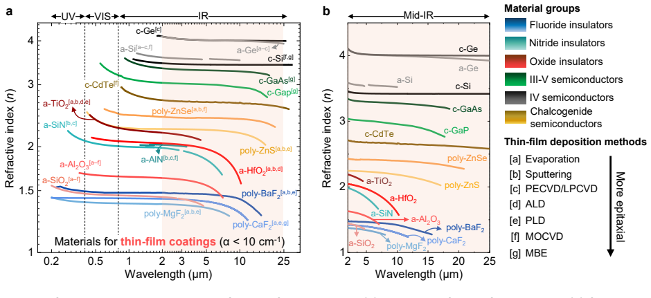
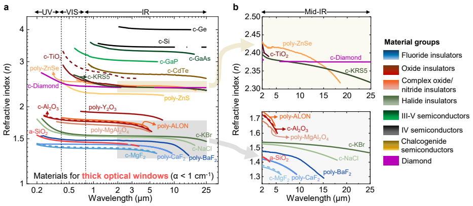
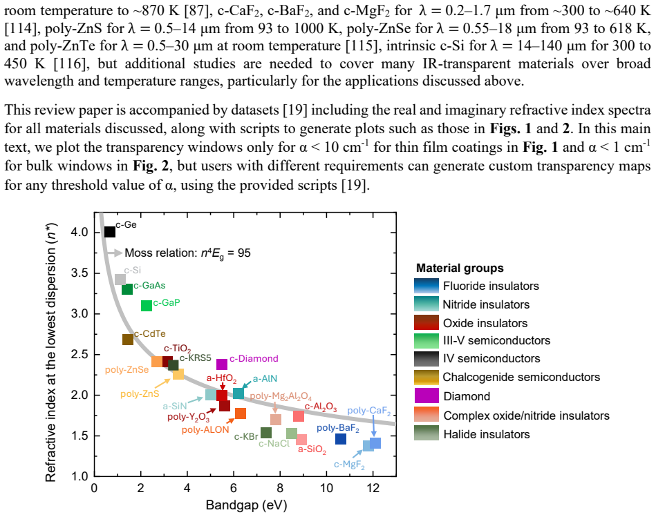
We summarized the room-temperature optical properties for infrared-transparent materials, defining transparency windows for two different applications: thin-film coatings (absorption coefficient α < 10 cm^{-1}) and windows (α < 1 cm^{-1}). The transparency requirements for thin films are substantially less stringent, enabling the use of many more optical materials for a given wavelength range.
What carries the argument
Absorption-coefficient thresholds (10 cm^{-1} for coatings, 1 cm^{-1} for windows) that mark the boundaries of usable transparency windows at each wavelength.
If this is right
- Designers can consider a larger set of candidate materials when the application is a thin film rather than a bulk window.
- Categorization by chemical group, crystallinity, and deposition technique directly narrows the search for compatible materials.
- Practical trade-offs such as chemical stability, thermal stability, hardness, and cost become part of the selection process alongside optical data.
- Regenerating the transparency maps with different thresholds or wavelengths is possible using the supplied datasets and scripts.
Where Pith is reading between the lines
- The compilation could shorten the material-search phase of mid-infrared optical design by providing a single reference map.
- Thresholds tuned to specific device geometries or operating temperatures would be a natural next use of the same data.
- Direct comparison of the compiled values against fabricated device performance would test whether the chosen cutoffs predict real-world behavior.
Load-bearing premise
The chosen absorption-coefficient thresholds of 10 cm^{-1} for coatings and 1 cm^{-1} for windows correctly separate materials that will work in practice from those that will not.
What would settle it
A laboratory measurement at a mid-infrared wavelength showing that a material listed as transparent under the coating threshold actually exhibits absorption above 10 cm^{-1}, or that a material below the window threshold exceeds 1 cm^{-1}.
Figures
read the original abstract
We summarized the room-temperature optical properties for infrared-transparent materials, defining transparency windows for two different applications: thin-film coatings (absorption coefficient $\alpha < 10 cm^{-1}$) and windows ($\alpha < 1 cm^{-1}$). The transparency requirements for thin films are substantially less stringent, enabling the use of many more optical materials for a given wavelength range. To make an easy-to-use reference, we categorized materials by chemical group, crystallinity, and typical deposition technique, and discussed practical pros and cons such as chemical and thermal stability, mechanical hardness, and cost. The datasets and plotting scripts are provided so that users can regenerate transparency-window maps for different applications. If you do optical design at infrared wavelengths, we recommend that you print out the figures and stick them on your wall.
Editorial analysis
A structured set of objections, weighed in public.
Referee Report
Summary. The manuscript compiles room-temperature optical properties of infrared-transparent materials and defines transparency windows using fixed absorption-coefficient thresholds: α < 10 cm^{-1} for thin-film coatings and α < 1 cm^{-1} for windows. Materials are grouped by chemical family, crystallinity, and typical deposition methods, with accompanying discussion of chemical/thermal stability, hardness, and cost. Open datasets and plotting scripts are supplied to allow regeneration of the maps under alternative criteria.
Significance. If the chosen thresholds align with real device requirements, the compilation provides a convenient, wall-chart-style reference for mid-IR material selection. The explicit release of datasets and scripts is a clear strength, enabling users to adapt the transparency maps to different loss tolerances or wavelengths.
major comments (1)
- [Abstract] Abstract and introduction: the transparency windows are defined solely by the fixed cutoffs α < 10 cm^{-1} (coatings) and α < 1 cm^{-1} (windows) without derivation from representative thicknesses (0.1–1 µm films, 1–10 mm windows) or explicit transmission calculations T = exp(−α d) that would quantify acceptable loss; this choice is load-bearing for the claimed practical utility of the defined windows.
Simulated Author's Rebuttal
We thank the referee for the constructive comment on justifying the transparency thresholds. We agree this strengthens the manuscript and will revise to include the requested derivations and transmission calculations.
read point-by-point responses
-
Referee: [Abstract] Abstract and introduction: the transparency windows are defined solely by the fixed cutoffs α < 10 cm^{-1} (coatings) and α < 1 cm^{-1} (windows) without derivation from representative thicknesses (0.1–1 µm films, 1–10 mm windows) or explicit transmission calculations T = exp(−α d) that would quantify acceptable loss; this choice is load-bearing for the claimed practical utility of the defined windows.
Authors: We acknowledge that the original manuscript presents the α thresholds without explicit derivation from thicknesses or T = exp(−α d) calculations. In the revised version we will add a concise justification in the introduction, using representative values (0.5 µm coatings, 5 mm windows) to show that α < 10 cm^{-1} yields T ≈ 99.95 % for coatings while α < 1 cm^{-1} yields T ≈ 60.7 % for windows—losses we consider acceptable for the respective applications. The supplied scripts already permit users to regenerate maps under any alternative criteria, so the fixed thresholds remain a convenient reference while the added calculations address the load-bearing concern. revision: yes
Circularity Check
No circularity: data compilation with fixed external thresholds
full rationale
The manuscript compiles room-temperature literature values for absorption coefficients of IR-transparent materials and applies two fixed, externally chosen thresholds (α < 10 cm^{-1} for coatings, α < 1 cm^{-1} for windows) to define transparency windows. No equations, fitting procedures, predictions, or derivations are present that could reduce to the input data by construction. The thresholds are stated as application-specific choices rather than derived quantities, and the work provides the underlying datasets for independent verification. This is a standard reference compilation with no load-bearing self-citation or self-definitional steps.
Axiom & Free-Parameter Ledger
Reference graph
Works this paper leans on
-
[1]
M. Hou, Y. Chen, J. Li, and F. Yi, “Single 5-centimeter- aperture metalens enabled intelligent lightweight mid-infrared thermographic camera,” Sci. Adv., vol. 10, no. 27, pp. 1–12, 2024, doi: 10.1126/sciadv.ado4847
-
[2]
S. Rosas, W. Adi, A. Beisenova, S. K. Biswas, F. Kuruoglu, H. Mei, M. A. Kats, D. A. Czaplewski, Y. S. Kivshar, and F. Yesilkoy, “Enhanced biochemical sensing with high-Q transmission resonances in free-standing membrane metasurfaces,” Optica, vol. 12, no. 2, pp. 178– 189, 2025, doi: 10.1364/optica.549393
-
[3]
Bidirectional mid-infrared communications between two identical macroscopic graphene fibres,
B. Fang, S. C. Bodepudi, F. Tian, X. Liu, D. Chang, S. Du, J. Lv, J. Zhong, H. Zhu, H. Hu, Y. Xu, Z. Xu, W. Gao, and C. Gao, “Bidirectional mid-infrared communications between two identical macroscopic graphene fibres,” Nat. Commun., vol. 11, 6368, 2020, doi: 10.1038/s41467-020- 20033-2
-
[4]
Mid-infrared quantum cascade lasers,
Y. Yao, A. J. Hoffman, and C. F. Gmachl, “Mid-infrared quantum cascade lasers,” Nat. Photonics, vol. 6, no. 7, pp. 432–439, 2012, doi: 10.1038/nphoton.2012.143
-
[5]
Metasurface-Enhanced Infrared Spectroscopy: An Abundance of Materials and Functionalities,
A. John-Herpin, A. Tittl, L. Kühner, F. Richter, S. H. Huang, G. Shvets, S.-H. Oh, and H. Altug, “Metasurface-Enhanced Infrared Spectroscopy: An Abundance of Materials and Functionalities,” Adv. Mater., vol. 35, no. 34, 2023, doi: 10.1002/adma.202110163
-
[6]
Nonlinear Group IV photonics based on silicon and germanium: From near-infrared to mid-infrared,
L. Zhang, A. M. Agarwal, L. C. Kimerling, and J. Michel, “Nonlinear Group IV photonics based on silicon and germanium: From near-infrared to mid-infrared,” Nanophotonics, vol. 3, no. 4–5, pp. 247–268, 2014, doi: 10.1515/nanoph-2013-0020
-
[7]
Optical materials for maximal nanophotonic response [Invited],
H. Shim, Z. Kuang, and O. Miller, “Optical materials for maximal nanophotonic response [Invited],” Opt. Mater. Express, vol. 10, no. 7, pp. 1561–1585, 2020, doi: 10.1364/ome.396419
-
[8]
P. Klocek (Ed.), Handbook of infrared optical materials (1st ed.), CRC Press, 1991, doi: 10.1201/9781315213996
-
[9]
The Correct Material for Infrared (IR) Applications
“The Correct Material for Infrared (IR) Applications.” [Online]. Available: https://www.edmundoptics.com/knowledge-center/application-notes/optics/the-correct-material- for-infrared- applications/?srsltid=AfmBOopmSOzptoVtDAjPteBRjVfk6sPoSl7tEouxtdsi32KHsmmwIzXm
-
[10]
What optical materials work best in the IR (infrared)?
“What optical materials work best in the IR (infrared)?” [Online]. Available: https://escooptics.com/blogs/news/what-optical-materials-work-best-in-the-ir-infrared
-
[11]
S. Yue, Y. Liu, R. Wang, Y. Hou, H. Shi, Y. Feng, Z. Wen, and Z. Zhang, “All-silicon polarization-independent broadband achromatic metalens designed for the mid-wave and long- wave infrared,” Opt. Express, vol. 31, no. 26, p. 44340, 2023, doi: 10.1364/oe.506471
-
[12]
Wide-Field-of-View, Large-Area Long-Wave Infrared Silicon Metalenses,
H. I. Lin, J. Geldmeier, E. Baleine, F. Yang, S. An, Y. Pan, C. Rivero-Baleine, T. Gu, J. Hu, “Wide-Field-of-View, Large-Area Long-Wave Infrared Silicon Metalenses,” ACS Photonics, vol. 11, no. 5, pp. 1943–1949, 2024, doi: 10.1021/acsphotonics.4c00013
-
[13]
J. S. Yu, S. Jung, J.-W. Cho, G.-T. Park, M. Kats, S.-K. Kim, E. Lee, “Ultrathin Ge-YF3 antireflective coating with 0.5% reflectivity on high-index substrate for long-wavelength infrared cameras,” Nanophotonics, vol. 13, no. 21, pp. 4067–4078, 2024, doi: 10.1515/nanoph-2024-0360. 12
-
[14]
Dynamically Tunable Membrane Metasurfaces for Infrared Spectroscopy
F. Kuruoglu, S. Rosas, J.-W. Cho, D. A. Czaplewski, Y. Kivshar, M. Kats and F. Yesilkoy, “Dynamically Tunable Membrane Metasurfaces for Infrared Spectroscopy,” pp. 1–15, 2025, doi:10.48550/arXiv.2506.10115
work page internal anchor Pith review Pith/arXiv arXiv doi:10.48550/arxiv.2506.10115 2025
-
[15]
L. Norder, S. Yin, M. H. J. de Jong, F. Stallone, H. Aydogmus, P. M. Sberna, M. A. Bessa, and R. A. Norte, “Pentagonal photonic crystal mirrors: scalable lightsails with enhanced acceleration via neural topology optimization,” Nat. Commun., vol. 16, 2753, pp. 1–11, 2025, doi: 10.1038/s41467-025-57749-y
-
[16]
J. Friedrich, W. von Ammon, and G. Müller, Czochralski Growth of Silicon Crystals, Second Edi., vol. 2. Elsevier B.V., 2015. doi: 10.1016/B978-0-444-63303-3.00002-X
-
[17]
Silicon on insulator material technology,
M. Bruel, “Silicon on insulator material technology,” Electron. Lett., vol. 31, no. 14, pp. 1201– 1202, 1995, doi: 10.1049/el:19950805
-
[18]
W. J. Tropf, M. E. Thomas, and P. Klocek, “Infrared optical materials,” Proc. SPIE, vol. 10286, pp. 102860A, 1992, doi: 10.1117/12.245197
-
[19]
J.-W. Cho, T. Kumar, H. Mei, M. A. Kats (2026). IR transparency window. Zenodo. https://doi.org/10.5281/zenodo.20187375
-
[20]
Nanometre optical coatings based on strong interference effects in highly absorbing media,
M. A. Kats, R. Blanchard, P. Genevet, and F. Capasso, “Nanometre optical coatings based on strong interference effects in highly absorbing media,” Nat. Mater., vol. 12, no. 1, pp. 20–24, 2013, doi: 10.1038/nmat3443
-
[21]
Free-standing thin film Ge single crystals grown by plasma‐ enhanced chemical vapor deposition,
R. A. Outlaw and P. Hopson Jr., “Free-standing thin film Ge single crystals grown by plasma‐ enhanced chemical vapor deposition,” J. Appl. Phys., vol. 55, pp. 1461–1463, 1984, doi: 10.1063/1.333401
-
[22]
Single-crystal germanium growth on amorphous silicon,
K. A. McComber, X. Duan, J. Liu, J. Michel, and L. C. Kimerling, “Single-crystal germanium growth on amorphous silicon,” Adv. Funct. Mater., vol. 22, no. 5, pp. 1049–1057, 2012, doi: 10.1002/adfm.201102015
-
[23]
D. Franta, D. Nečas, A. Giglia, P. Franta, and I. Ohlídal, “Universal dispersion model for characterization of optical thin films over wide spectral range: Application to magnesium fluoride,” Appl. Surf. Sci., vol. 421, pp. 424–429, 2017, doi: 10.1016/j.apsusc.2016.09.149
-
[24]
D. F. Bezuidenhout, “Calcium Fluoride (CaF2),” Handb. Opt. Constants Solids, vol. II, pp. 815– 835, 1997, doi: 10.1016/B978-012544415-6.50082-0
-
[25]
Optical constants of minerals and other materials from the millimeter to the ultraviolet, Contractor Report CRDEC-CR-88009,
M. R. Querry, “Optical constants of minerals and other materials from the millimeter to the ultraviolet, Contractor Report CRDEC-CR-88009, ” pp. 61–70, 1987
1987
-
[26]
Dielectric classification of crystal structures, ionization potentials, and band structures,
J. C. Phillips and J. A. Van Vechten, “Dielectric classification of crystal structures, ionization potentials, and band structures,” Phys. Rev. Lett., vol. 22, no. 14, pp. 705–708, 1969, doi: 10.1103/PhysRevLett.22.705
-
[27]
H. J. Lee, D. Wang, T. H. Kim, D.-H. Jung, T.-H. Kil, K.-S. Lee, H.-J. Choi, S.-H. Baek, E. Yoon, W. J. Choi, and J. M. Baik, “Wide-temperature (up to 100 °C) operation of thermostable vanadium oxide based microbolometers with Ti/MgF2 infrared absorbing layer for long wavelength infrared (LWIR) detection,” Appl. Surf. Sci., vol. 547, p. 149142, 2021, doi:...
-
[28]
Fluoride antireflection coatings for deep ultraviolet optics deposited by ion-beam sputtering,
T. Yoshida, K. Nishimoto, K. Sekine, and K. Etoh, “Fluoride antireflection coatings for deep ultraviolet optics deposited by ion-beam sputtering,” Appl. Opt., vol. 45, no. 7, pp. 1375–1379, 2006, doi: 10.1364/AO.45.001375
-
[29]
D. Franta, D. Nečas, I. Ohlídal, and A. Giglia, “Optical characterization of SiO2 thin films using universal dispersion model over wide spectral range,” Proc. SPIE Opt. Micro- Nanometrology VI, vol. 9890, p. 989014, 2016, doi: 10.1117/12.2227580
-
[30]
Dispersion model for optical thin films applicable in wide spectral range,
D. Franta, D. Nečas, I. Ohlídal, and A. Giglia, “Dispersion model for optical thin films applicable in wide spectral range,” Proc. SPIE Opt. Syst. Des. 2015 Opt. Fabr. Testing, Metrol. V, vol. 9628, p. 96281U, 2015, doi: 10.1117/12.2190104
-
[31]
D. Franta, J. Vohánka, and M. Čermák, “Universal dispersion model for characterization of optical thin films over a wide spectral range: application to hafnia,” Appl. Opt., vol. 54, no. 31, pp. 9108– 9119, 2015, doi: 10.1007/978-3-319-75325-6_3
-
[32]
Infrared lattice absorption in ionic and homopolar crystals,
M. Lax and E. Burstein, “Infrared lattice absorption in ionic and homopolar crystals,” Phys. Rev., vol. 97, no. 1, pp. 39–52, 1955, doi: 10.1103/PhysRev.97.39
-
[33]
Comparing amorphous silica, short-range-ordered silicates and silicic acid species by FTIR,
R. Ellerbrock, M. Stein, and J. Schaller, “Comparing amorphous silica, short-range-ordered silicates and silicic acid species by FTIR,” Sci. Rep., vol. 12, no. 1, pp. 1–8, 2022, doi: 10.1038/s41598-022-15882-4
-
[34]
J. Xu, S. Li, W. Zhang, S. Yan, C. Liu, X. Yuan, X. Ye, and H. Li, “The impact of deposition and annealing temperature on the growth properties and surface passivation of silicon dioxide films obtained by atomic layer deposition,” Appl. Surf. Sci., vol. 544, no. December 2020, p. 148889, 2021, doi: 10.1016/j.apsusc.2020.148889
-
[35]
Defect formation in thermal SiO2 by high- temperature annealing,
K. Hofmann, G. W. Rubloff, and R. A. McCorkle, “Defect formation in thermal SiO2 by high- temperature annealing,” Appl. Phys. Lett., vol. 49, no. 22, pp. 1525–1527, 1986, doi: 10.1063/1.97322
-
[36]
Directional Radiative Cooling via Exceptional Epsilon-Based Microcavities,
J.-W. Cho, Y.-J. Lee, J.-H. Kim, R. Hu, E. Lee, and S.-K. Kim, “Directional Radiative Cooling via Exceptional Epsilon-Based Microcavities,” ACS Nano, vol. 17, no. 11, pp. 10442–10451, 2023, doi: 10.1021/acsnano.3c01184
-
[37]
Broadband mid-infrared frequency comb generation in a Si3N4 microresonator,
K. Luke, Y. Okawachi, M. R. E. Lamont, A. L. Gaeta, M. Lipson, “Broadband mid-infrared frequency comb generation in a Si3N4 microresonator,” Opt. Lett., vol. 40, no. 21, pp. 4823–4826, 2015, doi: 10.1364/OL.40.004823
-
[38]
L. Y. Beliaev, E. Shkondin, A. V. Lavrinenko, and O. Takayama, “Optical, structural and composition properties of silicon nitride films deposited by reactive radio-frequency sputtering, low pressure and plasma-enhanced chemical vapor deposition,” Thin Solid Films, vol. 763, pp. 139568, 2022, doi: 10.1016/j.tsf.2022.139568
-
[39]
Structural, optical and electrical properties of Si-rich and N-rich PECVD silicon nitride films,
T. Al Moussi, C. O’Dalaigh, P. Raynaud, J. Esvan, P. Lambkin, R. Lakshmanan, B. Chen, and S. Diaham, “Structural, optical and electrical properties of Si-rich and N-rich PECVD silicon nitride films,” Sci. Rep., vol. 15, no. 1, pp. 1–14, 2025, doi: 10.1038/s41598-025-14296-2. 14
-
[40]
Low loss CMOS- compatible silicon nitride photonics utilizing reactive sputtered thin films,
A. Frigg, A. Boes, G. Ren, I. Abdo, D.-Y. Choi, S. Gees, and A. Mitchell, “Low loss CMOS- compatible silicon nitride photonics utilizing reactive sputtered thin films,” Opt. Express, vol. 27, no. 26, pp. 37795–37805, 2019, doi: 10.1364/oe.380758
-
[41]
Composition limited hydrogen effusion rate of a-SiNx:H passivation stack,
S. Jafari, J. Hirsch, D. Lausch, M. John, N. Bernhard, and S. Meyer, “Composition limited hydrogen effusion rate of a-SiNx:H passivation stack,” AIP Conf. Proc., vol. 2147, 2019, doi: 10.1063/1.5123853
-
[42]
T. Kumar, D. Feng, S. Yin, M. Mah, P. Lin, M. A. Fortman, G. R. Jaffe, C. Wan, H. Mei, Y. Xiao, R. Synowicki, R. J. Warzoha, V. W. Brar, J. J. Talghader, and M. A. Kats, “Self-Referencing Photothermal Common-Path Interferometry to Measure Absorption of Si3N4 Membranes for Laser-Light Sails,” ACS Photonics, vol. 12, no. 11, pp. 6381–6387, 2025, doi: 10.102...
-
[43]
Thickness-dependent optical properties of aluminum nitride films for mid-infrared wavelengths,
L. Y. Beliaev, E. Shkondin, A. V. Lavrinenko, and O. Takayama, “Thickness-dependent optical properties of aluminum nitride films for mid-infrared wavelengths,” J. Vac. Sci. Technol. A Vacuum, Surfaces, Film., vol. 39, no. 4, 2021, doi: 10.1116/6.0000884
-
[44]
H. Fu, X. Huang, H. Chen, Z. Lu, and Y. Zhao, “Fabrication and Characterization of Ultra-wide Bandgap AlN-Based Schottky Diodes on Sapphire by MOCVD,” IEEE J. Electron Devices Soc., vol. 5, no. 6, pp. 518–524, 2017, doi: 10.1109/JEDS.2017.2751554
-
[45]
Preparation of high-quality AlN on sapphire by high-temperature face-to-face annealing,
H. Miyake, C. H. Lin, K. Tokoro, and K. Hiramatsu, “Preparation of high-quality AlN on sapphire by high-temperature face-to-face annealing,” J. Cryst. Growth, vol. 456, pp. 155–159, 2016, doi: 10.1016/j.jcrysgro.2016.08.028
-
[46]
Full-Color Solar-Heat-Resistant Films Based on Nanometer Optical Coatings,
J.-W. Cho, E.-J. Lee, and S.-K. Kim, “Full-Color Solar-Heat-Resistant Films Based on Nanometer Optical Coatings,” Nano Lett., 2021, doi: 10.1021/acs.nanolett.1c04043
-
[47]
Anti-reflection coatings for highly anisotropic materials in the mid infrared,
H. Mei, J.-W. Cho, J.-S. Yu, H. Chen, S. Singh, B. Zhao, J. Ravichandran, S.-K. Kim, M. A. Kats, “Anti-reflection coatings for highly anisotropic materials in the mid infrared,” arXiv:2601.00558, doi: 10.48550/arXiv.2601.00558
-
[48]
E. D. Palik, “Cadmium Telluride (CdTe),” Handb. Opt. Constants Solids, vol. I, pp. 409–427, 1997, doi: 10.1016/B978-012544415-6.50017-0
-
[49]
Longwave infrared absorption and scatter properties of ZnS and ZnSe,
D. W. Blodgett, M. E. Thomas, D. V. Hahn, and S. G. Kaplan, “Longwave infrared absorption and scatter properties of ZnS and ZnSe,” Proc. SPIE Wind. Dome Technol. VIII, vol. 5078, p. 137, 2003, doi: 10.1117/12.487874
-
[50]
Investigation of cadmium alternatives in thin-film coatings,
S. J. Wakeham and G. J. Hawkins, “Investigation of cadmium alternatives in thin-film coatings,” Proc. SPIE Adv. Thin-Film Coatings Opt. Appl. III, vol. 6286, p. 62860C, 2006, doi: 10.1117/12.680349
-
[51]
Electrical and Optical Properties of γ-SnSe: A New Ultra-narrow Band Gap Material,
N. Zakay, A. Schlesinger, U. Argaman, L. Nguyen, N. Maman, B. Koren, M. Ozeri, G. Makov, Y. Golan, and D. Azulay, “Electrical and Optical Properties of γ-SnSe: A New Ultra-narrow Band Gap Material,” ACS Appl. Mater. Interfaces, vol. 15, no. 12, pp. 15668–15675, 2023, doi: 10.1021/acsami.2c22134. 15
-
[52]
Gallium Phosphide (GaP),
S. Adachi, “Gallium Phosphide (GaP),” in Optical Constants of Crystalline and Amorphous Semiconductors: Numerical Data and Graphical Information. Boston, MA: Kluwer Academic, Springer Science & Business Media, pp. 198–212, 1999
1999
-
[53]
E. D. Palik, “Gallium Arsenide (GaAs),” Handb. Opt. Constants Solids, vol. I, pp. 429–443, 1997, doi: 10.1016/b978-012544415-6.50018-2
-
[54]
III-V nitride based light-emitting devices,
S. Nakamura, “III-V nitride based light-emitting devices,” Solid State Commun., vol. 102, no. 2–3, pp. 237–243, 1997, doi: 10.1016/S0038-1098(96)00722-3
-
[55]
III-V compounds for solar cell applications,
A. W. Bett, F. Dimroth, G. Stollwerck, and O. V. Sulima, “III-V compounds for solar cell applications,” Appl. Phys. A Mater. Sci. Process., vol. 69, no. 2, pp. 119–129, 1999, doi: 10.1007/s003390050983
-
[56]
Fabrication of Single Crystal Gallium Phosphide Thin Films on Glass,
H. Emmer, C. T. Chen, R. Saive, D. Friedrich, Y. Horie, A. Arbabi, A. Faraon, and H. A. Atwaterm, “Fabrication of Single Crystal Gallium Phosphide Thin Films on Glass,” Sci. Rep., vol. 7, no. 1, pp. 2–7, 2017, doi: 10.1038/s41598-017-05012-w
-
[57]
GaAs Mid-IR Electrically Tunable Metasurfaces,
H. U. Chae, B. Shrewsbury, R. Ahsan, M. L. Povinelli, and R. Kapadia, “GaAs Mid-IR Electrically Tunable Metasurfaces,” Nano Lett., vol. 24, no. 8, pp. 2581–2588, 2024, doi: 10.1021/acs.nanolett.3c04687
-
[58]
Influence of Process Parameters on the RF Sputtered GaP Thin Films,
D. A. Mota, G. H. Chandra, J. Ventura, A. Guedes, and J. P. De Cruz, “Influence of Process Parameters on the RF Sputtered GaP Thin Films,” J. Mater. Sci. Technol., vol. 29, no. 9, pp. 821– 829, 2013, doi: 10.1016/j.jmst.2013.06.005
-
[59]
M. Imaizumi, M. Adachi, Y. Fujii, Y. Hayashi, T. Soga, T. Jimbo, M. Umeno, “Low-temperature growth of GaAs polycrystalline films on glass substrates for space solar cell application,” J. Cryst. Growth, vol. 221, pp. 688–692, 2000, doi: doi:10.1016/S0022-0248(00)00801-0
-
[60]
Temperature- dependent dispersion model of float zone crystalline silicon,
D. Franta, A. Dubroka, C. Wang, A. Giglia, J. Vohánka, P. Franta, and I. Ohlídal, “Temperature- dependent dispersion model of float zone crystalline silicon,” Appl. Surf. Sci., vol. 421, pp. 405– 419, 2017, doi: 10.1016/j.apsusc.2017.02.021
-
[61]
Infrared lattice absorption bands in germanium, silicon, and diamond,
R. J. Collins and H. Y. Fan, “Infrared lattice absorption bands in germanium, silicon, and diamond,” Phys. Rev., vol. 93, no. 4, pp. 674–678, 1954, doi: 10.1103/PhysRev.93.674
-
[62]
Fox, Optical Properties of Solids, 2nd ed
M. Fox, Optical Properties of Solids, 2nd ed. Oxford: Oxford University Press, 2010
2010
-
[63]
Advanced modeling for optical characterization of amorphous hydrogenated silicon films,
D. Franta, D. Nečas, L. Zajíčková, I. Ohlídal, and J. Stuchlík, “Advanced modeling for optical characterization of amorphous hydrogenated silicon films,” Thin Solid Films, vol. 541, pp. 12–16, 2013, doi: 10.1016/j.tsf.2013.04.129
-
[64]
Application of sum rule to the dispersion model of hydrogenated amorphous silicon,
D. Franta, D. Nečas, L. Zajíčková, I. Ohlídal, J. Stuchlík, and D. Chvostová, “Application of sum rule to the dispersion model of hydrogenated amorphous silicon,” Thin Solid Films, vol. 539, pp. 233–244, 2013, doi: 10.1016/j.tsf.2013.04.012
-
[65]
Woollam) and fitted using WVASE software
A 100-nm-thick a-Ge was deposited on a c-Si substrate by e-beam evaporation, and its optical constants were measured by IR-VASE (infrared variable-angle spectroscopic ellipsometry, J.A. Woollam) and fitted using WVASE software
-
[66]
R. F. Potter, “Germanium (Ge),” Handb. Opt. Constants Solids, vol. I, pp. 465–478, 1997, doi: 10.1016/B978-012544415-6.50020-0. 16
-
[67]
Broadband Light Extraction from Near-Surface NV Centers Using Crystalline-Silicon Antennas,
M. Kim, M. Zahedian, W. Wu, C. Fang, Z. Yu, R. A. Wambold, R. Vidrio, Y. Tong, S. Yin, D. A. Czaplewski, J. T. Choy, and M. A. Kats, “Broadband Light Extraction from Near-Surface NV Centers Using Crystalline-Silicon Antennas,” Nano Lett., vol. 25, no. 12, pp. 4659–4666, 2025, doi: 10.1021/acs.nanolett.4c04299
-
[68]
Infrared refractive index of diamond,
D. F. Edwards and E. Ochoa, “Infrared refractive index of diamond,” J. Opt. Soc. Am., vol. 71, no. 5, pp. 607–608, 1981, doi: 10.1364/josa.71.000607
-
[69]
Development of high-purity optical grade single-crystal CVD diamond for intracavity cooling,
A. M. Bennett, B. J. Wickham, H. K. Dhilon, Y. Chen, S. Webster, G. Turri, and M. Bass, “Development of high-purity optical grade single-crystal CVD diamond for intracavity cooling,” Proc. SPIE Solid State Lasers XXIII Technol. Devices, vol. 8959, p. 89590R, 2014, doi: 10.1117/12.2037811
-
[70]
E. D. Palik, “Potassium Bromide (KBr),” Handb. Opt. Constants Solids, vol. II, pp. 989–1004, 1997, doi: 10.1016/B978-012544415-6.50090-X
-
[71]
J. E. Eldridge and E. D. Palik, “Sodium chloride (NaCl),” Handb. Opt. Constants Solids, vol. I, pp. 775–793, 1997, doi: 10.1016/B978-012544415-6.50041-8
-
[72]
W. J. Tropf, “Cubic Thallium (I) Halides,” Handb. Opt. Constants Solids, vol. III, pp. 923–961, 1997, doi: 10.1016/B978-012544415-6.50140-0
-
[73]
Aluminum Oxynitride (ALON) Spinel,
W. J. Tropf and M. E. Thomas, “Aluminum Oxynitride (ALON) Spinel,” Handb. Opt. Constants Solids, vol. II, pp. 777–787, 1997, doi: 10.1016/B978-012544415-6.50079-0
-
[74]
Magnesium Aluminum Spinel (MgAl2O4),
W. J. Tropf and M. E. Thomas, “Magnesium Aluminum Spinel (MgAl2O4),” Handb. Opt. Constants Solids, vol. II, pp. 883–894a, 1997, doi: 10.1016/B978-012544415-6.50086-8
-
[75]
Optical Studies on Hot-Pressed Polycrystalline CaF2 With Clean Grain Boundaries,
E. Carnall, S. E. Hatch, and W. F. Parsons, “Optical Studies on Hot-Pressed Polycrystalline CaF2 With Clean Grain Boundaries,” Role Grain Boundaries Surfaces Ceram., pp. 165–173, 1966, doi: 10.1007/978-1-4899-6311-6_11
-
[76]
D. C. Harris, Materials for Infrared Windows and Domes: Properties and Performance. Bellingham, WA, USA: SPIE Press, 1999, doi: 10.1117/3.349896
-
[77]
Photonchina
“Photonchina.” [Online]. Available: https://www.photonchinaa.com/product/caf2/
-
[78]
FarfieldCrystal
“FarfieldCrystal”, [Online]. Available: https://fairfieldcrystal.com/the-strengths-of-magnesium- fluoride-in-uv-optics/
-
[79]
Barium Fluoride Windows
“Barium Fluoride Windows.” [Online]. Available: https://www.thorlabs.com/barium-fluoride- windows/?gad_source=1&gad_campaignid=21369512767&gbraid=0AAAAAD_iN3gAKfjqFLoc p77gvRhLQnPbE&gclid=CjwKCAjwwJzPBhBREiwAJfHRnZrM5wzmbe_H9uyTSL8FUsQMsd 040bAgbGiBeOpnAFW7uJt1X71fHRoCvwoQAvD_BwE&tabName=Overview
-
[80]
Calcium Fluoride Windows
“Calcium Fluoride Windows.” [Online]. Available: https://www.thorlabs.com/calcium-fluoride- windows?tabName=Overview
discussion (0)
Sign in with ORCID, Apple, or X to comment. Anyone can read and Pith papers without signing in.