Flux-trapping characterization for superconducting electronics using a cryogenic widefield N-V diamond microscope
Pith reviewed 2026-05-19 11:47 UTC · model grok-4.3
The pith
A cryogenic widefield microscope with NV centers in diamond images magnetic flux trapping in superconducting devices at micrometer scale.
A machine-rendered reading of the paper's core claim, the machinery that carries it, and where it could break.
Core claim
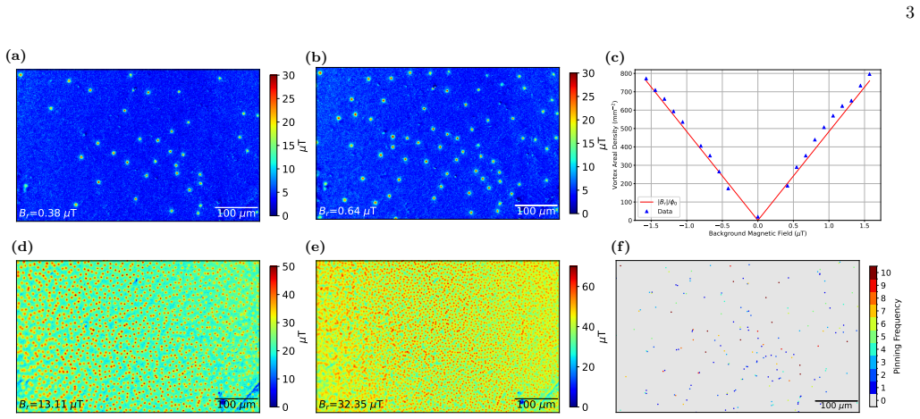
We present a cryogenic widefield NV-diamond magnetic microscope capable of rapid, micrometer-scale imaging of flux trapping in superconducting devices. Using this technique, we measure vortex expulsion fields in Nb thin films and patterned strips, revealing a crossover in expulsion behavior between 10 and 20 μm strip widths. The observed scaling agrees with theoretical models and suggests the influence of film defects on vortex expulsion dynamics.
What carries the argument
Cryogenic widefield NV-diamond magnetic microscope that maps stray magnetic fields from superconducting vortices through fluorescence collected from nitrogen-vacancy centers.
If this is right
- Rapid mapping of trapped flux across entire superconducting circuits becomes practical.
- Vortex expulsion fields exhibit a clear crossover with strip width that follows existing models.
- Film defects are implicated as the dominant factor setting expulsion dynamics in the measured range.
- High-throughput characterization supports systematic development of flux-mitigation designs.
Where Pith is reading between the lines
- The same widefield approach could be applied to other common superconductors such as aluminum or tantalum.
- Real-time imaging during temperature or current ramps might reveal vortex motion pathways directly.
- On-wafer testing of fabricated circuits could become routine for quality control in superconducting electronics.
- Width-dependent expulsion data may guide geometry choices that reduce flux noise in quantum devices.
Load-bearing premise
The vortex expulsion field values measured in the patterned niobium strips represent intrinsic material behavior rather than effects introduced by the microscope, sample mounting, or analysis steps.
What would settle it
Independent expulsion-field measurements on the same niobium strip widths performed with scanning Hall-probe microscopy or magneto-optical imaging that show no crossover near 10-20 micrometers would falsify the reported scaling behavior.
Figures


read the original abstract
Magnetic flux trapping is a significant hurdle limiting the reliability and scalability of superconducting electronics, yet tools for imaging flux vortices remain slow or insensitive. We present a cryogenic widefield NV-diamond magnetic microscope capable of rapid, micrometer-scale imaging of flux trapping in superconducting devices. Using this technique, we measure vortex expulsion fields in Nb thin films and patterned strips, revealing a crossover in expulsion behavior between $10$ and $20~\mu$m strip widths. The observed scaling agrees with theoretical models and suggests the influence of film defects on vortex expulsion dynamics. This instrument enables high-throughput magnetic characterization of superconducting materials and circuits, providing new insight for flux mitigation strategies in scalable superconducting electronics.
Editorial analysis
A structured set of objections, weighed in public.
Referee Report
Summary. The manuscript introduces a cryogenic widefield NV-diamond magnetic microscope for rapid, micrometer-scale imaging of magnetic flux trapping in superconducting devices. Using this instrument, the authors measure vortex expulsion fields in Nb thin films and patterned strips, reporting a crossover in expulsion behavior between 10 and 20 μm strip widths. The observed scaling is stated to agree with theoretical models and to indicate the influence of film defects on vortex dynamics.
Significance. If the central measurements are shown to be free of setup artifacts, the work would provide a practical high-throughput tool for characterizing flux trapping, directly addressing a key limitation in scaling superconducting electronics. The combination of cryogenic operation with widefield imaging offers a clear advance over slower scanning techniques for device-level diagnostics.
major comments (2)
- [Abstract / Results] Abstract and results: the reported crossover in vortex expulsion fields between 10 and 20 μm strip widths is presented without error bars, statistical uncertainties, or details of the number of devices measured. This omission makes it impossible to assess whether the claimed agreement with theoretical models is statistically significant or whether the crossover could arise from measurement variability.
- [Methods] Methods: the description of the cryogenic widefield NV setup does not include an explicit calibration curve for NV response at the operating temperature or quantitative bounds on sensor-sample distance and mounting-induced strain. Without these controls, the width-dependent expulsion fields cannot be confidently attributed to intrinsic material or defect effects rather than microscope-specific field inhomogeneity or resolution limits.
minor comments (2)
- [Figures] Figure captions should explicitly state the number of independent measurements or devices averaged for each data point.
- [Methods] Notation for NV orientation averaging and its effect on the extracted B-field magnitude should be clarified in the methods.
Simulated Author's Rebuttal
We thank the referee for their constructive review and positive assessment of the work's potential significance. We address the two major comments point by point below, providing the strongest honest defense of the manuscript while committing to revisions where the concerns are valid.
read point-by-point responses
-
Referee: [Abstract / Results] Abstract and results: the reported crossover in vortex expulsion fields between 10 and 20 μm strip widths is presented without error bars, statistical uncertainties, or details of the number of devices measured. This omission makes it impossible to assess whether the claimed agreement with theoretical models is statistically significant or whether the crossover could arise from measurement variability.
Authors: We agree that the absence of error bars, uncertainties, and device statistics weakens the presentation of the crossover result. In the revised manuscript we will add error bars (standard deviation from repeated measurements) to the expulsion-field data, report the number of devices measured per width (N ≥ 5), and include a brief statistical comparison to the theoretical prediction. These additions will allow readers to evaluate the significance of the observed crossover directly from the data. revision: yes
-
Referee: [Methods] Methods: the description of the cryogenic widefield NV setup does not include an explicit calibration curve for NV response at the operating temperature or quantitative bounds on sensor-sample distance and mounting-induced strain. Without these controls, the width-dependent expulsion fields cannot be confidently attributed to intrinsic material or defect effects rather than microscope-specific field inhomogeneity or resolution limits.
Authors: We acknowledge that the methods section lacked these quantitative controls. The revised manuscript will incorporate an NV calibration curve acquired at the base temperature of the cryostat, together with measured sensor-sample distances (obtained from optical focus and interferometric checks) and upper-bound estimates of mounting strain derived from the mechanical fixture design. These additions will support the claim that the width-dependent behavior reflects intrinsic vortex dynamics rather than instrumental artifacts. revision: yes
Circularity Check
No circularity: experimental imaging results compared to external models
full rationale
The paper describes construction and use of a cryogenic widefield NV microscope for direct imaging of flux vortices in Nb devices, followed by measurement of expulsion fields in patterned strips. Results are presented as raw observations that are then compared to pre-existing theoretical models from the literature. No equations, fitted parameters, predictions, or derivations are described that reduce to the paper's own inputs by construction. No self-citation chains are invoked to justify uniqueness or ansatzes. The work is self-contained as an experimental characterization study.
Axiom & Free-Parameter Ledger
axioms (1)
- domain assumption Standard models of vortex expulsion in thin superconducting strips apply to the Nb films studied.
Lean theorems connected to this paper
-
IndisputableMonolith/Foundation/AlexanderDuality.leanalexander_duality_circle_linking unclear?
unclearRelation between the paper passage and the cited Recognition theorem.
We measure vortex expulsion fields in Nb thin films and patterned strips, revealing a crossover in expulsion behavior between 10 and 20 µm strip widths. The observed scaling agrees with theoretical models...
What do these tags mean?
- matches
- The paper's claim is directly supported by a theorem in the formal canon.
- supports
- The theorem supports part of the paper's argument, but the paper may add assumptions or extra steps.
- extends
- The paper goes beyond the formal theorem; the theorem is a base layer rather than the whole result.
- uses
- The paper appears to rely on the theorem as machinery.
- contradicts
- The paper's claim conflicts with a theorem or certificate in the canon.
- unclear
- Pith found a possible connection, but the passage is too broad, indirect, or ambiguous to say the theorem truly supports the claim.
Forward citations
Cited by 2 Pith papers
-
Wide-field magnetic imaging of shielding-current-driven vortex rearrangement under local heating using diamond quantum sensors
Wide-field NV imaging captured real-time rearrangement of vortices in an NbN film driven by shielding currents under local laser heating.
-
Mitigation of Magnetic Flux Trapping in Superconducting Electronics Using Moats
Systematic tests show high-aspect-ratio slit moats best sequester flux in shielded environments below 1 microtesla, yet vortices still pin at material defects so moats alone are insufficient.
Reference graph
Works this paper leans on
- [1]
-
[2]
A. I. Braginski, Journal of Superconductivity and Novel Magnetism 32, 23 (2019)
work page 2019
-
[3]
R. Bairamkulov and G. De Micheli, IEEE Circuits and Systems Magazine 24, 16 (2024)
work page 2024
-
[4]
W. Chen, A. Rylyakov, V. Patel, J. Lukens, and K. Likharev, IEEE Transactions on Applied Supercon- ductivity 9, 3212 (1999)
work page 1999
-
[5]
V. K. Semenov and M. M. Khapaev, IEEE Transactions on Applied Superconductivity 26, 1 (2016)
work page 2016
-
[6]
S. Narayana, Y. A. Polyakov, and V. K. Semenov, IEEE Transactions on Applied Superconductivity 19, 640 (2009)
work page 2009
-
[7]
I. S. Veshchunov, W. Magrini, S. V. Mironov, A. G. Godin, J.-B. Trebbia, A. I. Buzdin, P. Tamarat, and B. Lounis, Nature Communications 7, 12801 (2016)
work page 2016
-
[8]
C.-S. Lee, B. Janko, I. Derenyi, and A.-L. Barab´ asi, Nature 400, 337 (1999)
work page 1999
-
[9]
E. B. Golden, N. A. Parmar, V. K. Semenov, and S. K. Tolpygo, IEEE Transactions on Applied Superconductiv- ity 35, 1 (2025)
work page 2025
-
[10]
V. K. Semenov, Y. A. Polyakov, and S. K. Tolpygo, IEEE Transactions on Applied Superconductivity 27, 1 (2017)
work page 2017
-
[11]
M. Jeffery, T. Van Duzer, J. R. Kirtley, and M. B. Ketchen, Applied Physics Letters 67, 1769 (1995)
work page 1995
-
[12]
G. Stan, S. B. Field, and J. M. Martinis, Phys. Rev. Lett. 92, 097003 (2004)
work page 2004
-
[13]
S. Ooi, M. Tachiki, T. Mochiku, H. Ito, T. Kubo, A. Kikuchi, S. Arisawa, and K. Umemori, Phys. Rev. B 111, 094519 (2025)
work page 2025
- [14]
-
[15]
M. Pelliccione, A. Jenkins, P. Ovartchaiyapong, C. Reetz, E. Emmanouilidou, N. Ni, and A. C. Bleszynski Jayich, Nature Nanotechnology 11, 700 (2016)
work page 2016
- [16]
-
[17]
V. M. Acosta, L. S. Bouchard, D. Budker, R. Folman, T. Lenz, P. Maletinsky, D. Rohner, Y. Schlussel, and L. Thiel, Journal of Superconductivity and Novel Mag- netism 32, 85 (2019)
work page 2019
-
[18]
Y. Schlussel, T. Lenz, D. Rohner, Y. Bar-Haim, L. Bougas, D. Groswasser, M. Kieschnick, E. Rozenberg, L. Thiel, A. Waxman, J. Meijer, P. Maletinsky, D. Bud- ker, and R. Folman, Phys. Rev. Applied 10, 034032 (2018)
work page 2018
-
[19]
S. Nishimura, T. Kobayashi, D. Sasaki, T. Tsuji, T. Iwasaki, M. Hatano, K. Sasaki, and K. Kobayashi, Applied Physics Letters 123, 112603 (2023)
work page 2023
-
[20]
D. R. Glenn, R. R. Fu, P. Kehayias, D. Le Sage, E. A. Lima, B. P. Weiss, and R. L. Walsworth, Geochemistry, Geophysics, Geosystems 18, 3254 (2017)
work page 2017
-
[21]
N. Wang, C.-F. Liu, J.-W. Fan, X. Feng, W.-H. Leong, A. Finkler, A. Denisenko, J. Wrachtrup, Q. Li, and R.-B. Liu, Phys. Rev. Res. 4, 013098 (2022)
work page 2022
-
[22]
S. Lourette, A. Jarmola, V. M. Acosta, A. G. Birdwell, D. Budker, M. W. Doherty, T. Ivanov, and V. S. Mali- novsky, Phys. Rev. Appl. 19, 064084 (2023)
work page 2023
-
[23]
Additional details are included in the supplemental ma- terial
-
[24]
S. J. Karlson, P. Kehayias, J. M. Schloss, A. C. Maccabe, A. Libson, D. F. Phillips, G. Wang, P. Cappellaro, and D. A. Braje, Phys. Rev. Appl. 22, 064051 (2024)
work page 2024
-
[25]
S. K. Tolpygo, V. Bolkhovsky, T. J. Weir, A. Wynn, D. E. Oates, L. M. Johnson, and M. A. Gouker, IEEE Transactions on Applied Superconductivity 26, 1 (2016)
work page 2016
-
[26]
S. Van der Walt, J. L. Sch¨ onberger, J. Nunez-Iglesias, F. Boulogne, J. D. Warner, N. Yager, E. Gouillart, and T. Yu, PeerJ 2, e453 (2014)
work page 2014
- [27]
-
[28]
K. H. Kuit, J. R. Kirtley, W. van der Veur, C. G. Mole- naar, F. J. G. Roesthuis, A. G. P. Troeman, J. R. Clem, H. Hilgenkamp, H. Rogalla, and J. Flokstra, Phys. Rev. B 77, 134504 (2008)
work page 2008
-
[29]
Likharev, Radiophysics and Quantum Electronics 14, 722 (1971)
K. Likharev, Radiophysics and Quantum Electronics 14, 722 (1971)
work page 1971
-
[30]
A. L. Fetter, Physical Review B 22, 1200 (1980)
work page 1980
- [31]
-
[32]
K. H. Kuit, J. R. Kirtley, J. R. Clem, H. Rogalla, and J. Flokstra, IEEE Transactions on Applied Superconduc- tivity 19, 3537 (2009)
work page 2009
-
[33]
J. M. Kosterlitz and D. J. Thouless, Journal of Physics C: Solid State Physics 6, 1181 (1973)
work page 1973
- [34]
-
[35]
Maksimova, Physics of the Solid State40, 1607 (1998)
G. Maksimova, Physics of the Solid State40, 1607 (1998)
work page 1998
-
[36]
J. Kirtley, Reports on Progress in Physics 73, 126501 (2010). 7 APPENDIX Appendix: Microscope Apparatus—In this CW-ODMR spectroscopy setup, the NV layer is continuously op- tically pumped into the strong-fluorescence mS = 0 ground-state sublevel, while a probe MW field drives transitions to the weaker-fluorescence mS = ±1 sub- levels. Local magnetic field...
work page 2010
discussion (0)
Sign in with ORCID, Apple, or X to comment. Anyone can read and Pith papers without signing in.