Plasma Etch Process Optimization for Photonic-Grade Diamond-on-Insulator Substrates and Thickness Evaluation using Colorimetry
Pith reviewed 2026-06-26 16:02 UTC · model grok-4.3
The pith
A plasma etch thins bonded diamond membranes to 300 nm thickness for photonic-grade DOI substrates.
A machine-rendered reading of the paper's core claim, the machinery that carries it, and where it could break.
Core claim
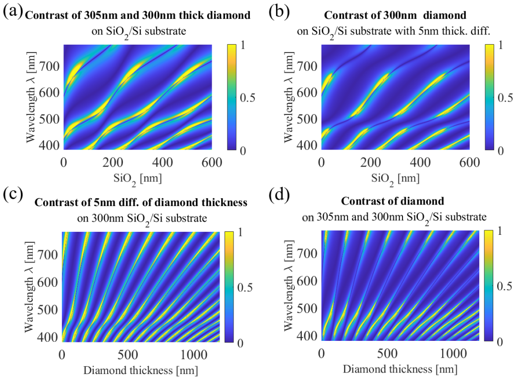
An ICP-RIE plasma etch thins a 10 μm (100) SCD membrane bonded to SiO₂/Si into a DOI substrate with diamond thickness ≤300 nm over 0.5 × 0.5 mm², roughness <0.5 nm, and intact interface, from which free-standing photonic chiplets are fabricated via two-step lithography; colorimetry on SiO₂ enables thickness extrapolation at 5 nm resolution matching WLI.
What carries the argument
The ICP-RIE plasma etch recipe that thins diamond while preserving the bonding interface and controlling surface quality.
If this is right
- Diamond photonic chiplets can be fabricated directly on the DOI using standard lithography without complex transfer or under-etching.
- The colorimetric method provides automatic thickness evaluation from microscope images with 5 nm resolution.
- The approach enables large-area photonic-grade DOI substrates for integration with manufacturing processes.
- Free-standing chiplets support modular quantum systems.
Where Pith is reading between the lines
- The thinning technique could extend to other diamond thicknesses or substrate sizes for broader quantum photonic applications.
- Colorimetry might serve as a quick validation tool in production lines for various thin-film materials.
- Integration with existing semiconductor processes becomes more feasible for diamond-based quantum devices.
Load-bearing premise
The ICP-RIE recipe preserves diamond bonding and provides sufficient micromasking and surface-quality control without damaging the interface or introducing defects.
What would settle it
Observation of bonding interface damage, surface roughness above 0.5 nm, or thickness measurements differing by more than 5 nm between colorimetry and white-light interferometry after etching.
Figures


read the original abstract
Diamond color-center qubits integrated with photonic circuits can be initialized, manipulated, entangled, and read individually with high fidelity, making them attractive for large-scale modular quantum computers, quantum networks, and distributed quantum sensing. However, the limited size of heteroepitaxially grown single-crystal diamond (SCD) and photonic-grade diamond-on-insulator (DOI) substrates remains a challenge for integration with existing manufacturing processes. Here, we develop a plasma etch recipe to thin direct-bonded (100) SCD membranes (<50 $\mu$m) into large-area, thin-film DOI substrates, and demonstrate free-standing photonic chiplets fabricated from the resulting DOI. The ICP-RIE recipe preserves diamond bonding, provides sufficient micromasking and surface-quality control, and enables thin-film DOI manufacture. We thin a 10 $\mu$m diamond plate bonded to SiO$_2$/Si and obtain a photonic-grade DOI substrate with diamond thickness $\leq$300 nm. The DOI film is around 300 nm thick over 0.5 $\times$ 0.5 mm$^2$, with surface roughness < 0.5 nm, while the bonding interface remains intact. Diamond photonic chiplets are fabricated on this DOI substrate using a standard two-step lithography process, without complex thin-film transfer, under-etching, or pedestal formation. We also present a colorimetric study of diamond visibility on SiO$_2$ and quantify color differences across thicknesses in common colorimetric spaces. This analysis enables automatic diamond-thickness extrapolation from standard optical microscope images with 5 nm resolution, in good agreement with white-light interferometry (WLI) measurements. The DOI substrate and colorimetric thickness-evaluation method provide an effective fabrication platform and reliable validation route for scalable manufacturing of diamond nanophotonic devices, opening a path toward large-scale integrated quantum systems.
Editorial analysis
A structured set of objections, weighed in public.
Referee Report
Summary. The manuscript describes the development of an ICP-RIE plasma etch recipe to thin direct-bonded (100) SCD membranes (<50 μm) bonded to SiO₂/Si into photonic-grade DOI substrates with diamond thickness ≤300 nm. It reports achieving this over 0.5 × 0.5 mm² areas with surface roughness <0.5 nm while preserving the bonding interface, followed by fabrication of free-standing photonic chiplets via standard lithography. A colorimetric method for diamond thickness evaluation on SiO₂ is also presented, claiming 5 nm resolution and agreement with white-light interferometry (WLI) measurements.
Significance. If substantiated with full process details and quantitative data, the work would provide a practical route to scalable DOI substrates for diamond color-center quantum photonics, avoiding complex thin-film transfer steps. The colorimetric thickness tool could enable simple, microscope-based validation in fabrication workflows. The experimental demonstration addresses a recognized bottleneck in diamond nanophotonics manufacturing.
major comments (3)
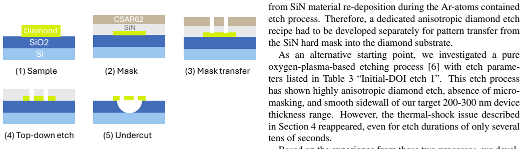
- [Methods] Methods section: No specific ICP-RIE parameters (gas flows, chamber pressure, RF/ICP powers, etch duration, or temperature) are reported, which directly undermines the central claim that a reproducible recipe achieves the stated thinning to ≤300 nm while preserving bonding and surface quality.
- [Results] Results on thickness and roughness: The claims of ≤300 nm thickness over 0.5 × 0.5 mm² and roughness <0.5 nm lack supporting data tables, AFM/WLI maps, error bars, or yield statistics across multiple samples or locations, making it impossible to assess uniformity or photonic-grade suitability.
- [Colorimetry] Colorimetry section: The stated 5 nm resolution and agreement with WLI are asserted without quantitative validation (e.g., no calibration curve, residual error analysis, or comparison table), which is load-bearing for the proposed automatic thickness extrapolation method.
minor comments (2)
- [Abstract] The abstract and text use 'photonic-grade' without defining the metric (e.g., specific loss or defect density thresholds) against which the substrate is evaluated.
- [Figures] Figure captions and axis labels for any thickness or roughness data should explicitly state measurement technique, number of samples, and uncertainty.
Simulated Author's Rebuttal
We thank the referee for the constructive feedback and positive evaluation of the work's significance for diamond nanophotonics. We address each major comment below and commit to revisions that strengthen the manuscript's reproducibility and quantitative support.
read point-by-point responses
-
Referee: [Methods] Methods section: No specific ICP-RIE parameters (gas flows, chamber pressure, RF/ICP powers, etch duration, or temperature) are reported, which directly undermines the central claim that a reproducible recipe achieves the stated thinning to ≤300 nm while preserving bonding and surface quality.
Authors: We agree that explicit process parameters are required for reproducibility. The original manuscript focused on the overall process flow and outcomes; we will add a detailed table in the revised Methods section listing all ICP-RIE parameters including gas flows, chamber pressure, RF/ICP powers, etch duration, and temperature. revision: yes
-
Referee: [Results] Results on thickness and roughness: The claims of ≤300 nm thickness over 0.5 × 0.5 mm² and roughness <0.5 nm lack supporting data tables, AFM/WLI maps, error bars, or yield statistics across multiple samples or locations, making it impossible to assess uniformity or photonic-grade suitability.
Authors: The reported values derive from our measurements, but we acknowledge the need for more comprehensive presentation. In revision we will include representative AFM and WLI maps, a data table with thickness uniformity and roughness statistics from multiple locations and samples, error bars, and available yield information. revision: yes
-
Referee: [Colorimetry] Colorimetry section: The stated 5 nm resolution and agreement with WLI are asserted without quantitative validation (e.g., no calibration curve, residual error analysis, or comparison table), which is load-bearing for the proposed automatic thickness extrapolation method.
Authors: We agree that quantitative validation is essential. We will add a calibration curve, residual error analysis, and a direct comparison table between colorimetric thickness predictions and WLI measurements to the revised Colorimetry section to substantiate the claimed resolution and agreement. revision: yes
Circularity Check
No significant circularity: purely experimental demonstration
full rationale
The manuscript describes an experimental ICP-RIE thinning process for bonded diamond membranes, achieving specified thickness and roughness metrics, followed by chiplet fabrication and a colorimetric thickness-evaluation method validated against WLI. No equations, derivations, fitted models presented as predictions, or self-citation chains appear in the abstract or described claims. The colorimetric analysis is an empirical quantification and extrapolation tool, not a self-referential prediction. The work is self-contained against external benchmarks (WLI measurements) with no load-bearing steps that reduce to inputs by construction.
Axiom & Free-Parameter Ledger
Reference graph
Works this paper leans on
-
[1]
C. M. Knaut, A. Suleymanzade, Y .-C. Wei, D. R. Assump- cao, P.-J. Stas, Y . Q. Huan, B. Machielse, E. N. Knall, M. Sutula, G. Baranes, N. Sinclair, C. De-Eknamkul, D. S. Levonian, M. K. Bhaskar, H. Park, M. Lon ˇcar, M. D. Lukin, Entanglement of nanophotonic quantum memory nodes in a telecom network, Nature 629 (8012) (2024) 573–578.doi:10.1038/s41586-02...
-
[2]
M. Xu, D. Wang, K. Fu, D. H. Mudiyanselage, H. Fu, Y . Zhao, A review of ultrawide bandgap materials: prop- erties, synthesis and devices, Oxford Open Materials Sci- ence 2 (1) (2022) itac004.doi:10.1093/oxfmat/ita c004
-
[3]
I. Aharonovich, A. D. Greentree, S. Prawer, Diamond photonics, Nature Photonics 5 (7) (2011) 397 – 405, 10.1038/nphoton.2011.54.doi:10.1038/nphoton. 2011.54
work page doi:10.1038/nphoton.2011.54.doi:10.1038/nphoton 2011
-
[4]
Prawer, I
S. Prawer, I. Aharonovich, Quantum Information Process- ing with Diamond: Principles and Applications, 1st Edi- tion, Woodhead Publishing, Limited, 2018
2018
-
[5]
Material platforms for spin-based photonic quantum technologies
M. Atatüre, D. Englund, N. Vamivakas, S.-Y . Lee, J. Wrachtrup, Material platforms for spin-based photonic quantum technologies, Nature Reviews Materials 491 (2018) 421.doi:10.1038/s41578-018-0008-9
-
[6]
M. Ruf, N. H. Wan, H. Choi, D. Englund, R. Hanson, Quantum networks based on color centers in diamond, Journal of Applied Physics 130 (7) (2021) 070901.doi: 10.1063/5.0056534
-
[7]
G. Perez, A. Maréchal, G. Chicot, P. Lefranc, P.-O. Jean- nin, D. Eon, N. Rouger, Diamond semiconductor perfor- mances in power electronics applications, Diamond and Related Materials 110 (2020) 108154.d o i : h t t p s : //doi.org/10.1016/j.diamond.2020.108154. URLhttps://www.sciencedirect.com/science/ article/pii/S092596352030707X
-
[8]
Donato, N
N. Donato, N. Rouger, J. Pernot, G. Longobardi, F. Udrea, Diamond power devices: state of the art, modelling, fig- ures of merit and future perspective, Journal of Physics D: Applied Physics 53 (9) (2020) 093001.doi:10.1088/ 1361-6463/ab4eab
2020
-
[9]
M. M. Hasan, C. Wang, N. Pala, M. Shur, Diamond for high-power, high-frequency, and terahertz plasma wave electronics, Nanomaterials 14 (5) (2024).doi:10.3390/ nano14050460. URLhttps://www.mdpi.com/2079-4991/14/5/460
2024
-
[10]
J. Liang, N. Shigekawa, Direct bonding of diamond and dissimilar materials for fabricating high performace power devices, in: S. Mandal, N. Yang (Eds.), Novel As- pects of Diamond II Science and Technology, Topics in Applied Physics, 2024, pp. 237–268.doi:10.1007/97 8-3-031-47556-6_9
work page doi:10.1007/97 2024
-
[11]
M. Angelone, C. Verona, Properties of diamond-based neutron detectors operated in harsh environments, Jour- nal of Nuclear Engineering 2 (4) (2021) 422–470.doi: 10.3390/jne2040032. URLhttps://www.mdpi.com/2673-4362/2/4/32
-
[12]
V . K. Khanna, Diamond electronics for ultra-hot environ- ments, 2053-2563, IOP Publishing, 2023, Ch. 10, pp. 10– 1 to 10–33.doi:10.1088/978-0-7503-5072-3ch10. URLhttps://dx.doi.org/10.1088/978-0-7503- 5072-3ch10
-
[13]
H. Umezawa, Diamond semiconductor devices for harsh environmental applications, in: 2022 6th IEEE Elec- tron Devices Technology & Manufacturing Conference 17 (EDTM), 2022, pp. 297–299.doi:10.1109/EDTM53 872.2022.9798392
-
[14]
P. Latawiec, V . Venkataraman, M. J. Burek, B. J. M. Haus- mann, I. Bulu, M. Lon ˇcar, On-chip diamond raman laser, Optica 2 (11) (2015) 924–928.arXiv:1509.00373, doi:10.1364/optica.2.000924
work page internal anchor Pith review Pith/arXiv arXiv doi:10.1364/optica.2.000924 2015
-
[15]
B. J. M. Hausmann, I. Bulu, V . Venkataraman, P. Deotare, M. Lonˇcar, Diamond nonlinear photonics, Nature Photon- ics 8 (5) (2014) 369–374.doi:10.1038/nphoton.20 14.72
-
[16]
R. Katsumi, K. Takada, F. Jelezko, T. Yatsui, Recent progress in hybrid diamond photonics for quantum in- formation processing and sensing, Communications En- gineering 4 (1) (2025) 85, publisher: Nature Publishing Group.doi:10.1038/s44172-025-00398-2. URLhttps://www.nature.com/articles/s44172- 025-00398-2
-
[17]
C. Bradac, W. Gao, J. Forneris, M. E. Trusheim, I. Aharonovich, Quantum nanophotonics with group IV defects in diamond, Nature Communications 10 (1) (2019) 5625.doi:10.1038/s41467-019-13332-w
-
[18]
E. Janitz, M. K. Bhaskar, L. Childress, Cavity quantum electrodynamics with color centers in diamond, Optica 7 (10) (2020) 1232–1252, publisher: Optica Publishing Group.doi:10.1364/OPTICA.398628. URLhttps://opg.optica.org/optica/abstract .cfm?uri=optica-7-10-1232
-
[19]
S. Pezzagna, J. Meijer, Quantum computer based on color centers in diamond, Applied Physics Reviews 8 (1) (2021) 011308.doi:10.1063/5.0007444
-
[20]
N. Mizuochi, T. Makino, H. Kato, D. Takeuchi, M. Ogura, H. Okushi, M. Nothaft, P. Neumann, A. Gali, F. Jelezko, J. Wrachtrup, S. Yamasaki, Electrically driven single- photon source at room temperature in diamond, Nature Photonics 6 (5) (2012) 299–303.doi:10.1038/nphoto n.2012.75
-
[21]
C. G. Torun, M. Gokce, T. K. Bracht, M. I. Monsalve, S. Benbouabdellah, O. O. Nacitarhan, M. E. Stucki, D. B. Alvaro, M. L. Markham, T. Pregnolato, J. H. D. Munns, G. Pieplow, D. E. Reiter, T. Schröder, SUPER and fem- tosecond spin-conserving coherent excitation of a tin- vacancy color center in diamond, Nature Communications 17 (1) (2026) 2154.doi:10.103...
-
[22]
Nitrogen-Vacancy Centers in Diamond: Nanoscale Sensors for Physics and Biology
R. Schirhagl, K. Chang, M. Loretz, C. L. Degen, Nitrogen-vacancy centers in diamond: Nanoscale sensors for physics and biology, dx.doi.org 65 (1) (2014) 83 – 105. doi:10.1146/annurev-physchem-040513-103659. URLh t t p s : / / d o i . o r g / 1 0 . 1 1 4 6 / a n n u r e v - physchem-040513-103659
-
[23]
E. V . Levine, M. J. Turner, P. Kehayias, C. A. Hart, N. Langellier, R. Trubko, D. R. Glenn, R. R. Fu, R. L. Walsworth, Principles and techniques of the quantum di- amond microscope, Nanophotonics 8 (11) (2019) 1945– 1973.doi:10.1515/nanoph-2019-0209
-
[24]
Y . Wang, W. Zhang, H. Chai, Z. Zhang, S. Lin, X. Qin, J. Du, Fully integrated quantum magnetometer based on nitrogen-vacancy centers, Physical Review Applied 23 (3) (2025) 034008.doi:10.1103/physrevapplied.23. 034008
-
[25]
I. Varveris, G. D. Aliberti, F. J. Barzilaij, Z. Jin, S. A. v. Rijs, Q. Dong, D. Brinks, S. Nur, R. Ishihara, Toward a CMOS-integrated quantum diamond biosensor based on NV centers (2026).arXiv:2602.20437,doi:10.485 50/arxiv.2602.20437. URLhttps://arxiv.org/abs/2602.20437
arXiv 2026
-
[26]
G. D. Fuchs, G. Burkard, P. V . Klimov, D. D. Awschalom, A quantum memory intrinsic to single nitrogen–vacancy centres in diamond, Nature Physics 7 (10) (2011) 789– 793.doi:10.1038/nphys2026
-
[27]
P. C. Maurer, G. Kucsko, C. Latta, L. Jiang, N. Y . Yao, S. D. Bennett, F. Pastawski, D. Hunger, N. Chisholm, M. Markham, D. J. Twitchen, J. I. Cirac, M. D. Lukin, Room-temperature quantum bit memory exceeding one second, Science 336 (6086) (2012) 1283 – 1286.doi: 10.1126/science.1220513. URLhttp://science.sciencemag.org/content/3 36/6086/1283
-
[28]
C. E. Bradley, S. W. d. Bone, P. F. W. Möller, S. Baier, M. J. Degen, S. J. H. Loenen, H. P. Bartling, M. Markham, D. J. Twitchen, R. Hanson, D. Elkouss, T. H. Taminiau, Robust quantum-network memory based on spin qubits in isotopically engineered diamond, npj Quantum Informa- tion 8 (1) (2022) 122.doi:10.1038/s41534- 022- 00637-w
-
[29]
M. Pompili, S. L. N. Hermans, S. Baier, H. K. C. Beukers, P. C. Humphreys, R. N. Schouten, R. F. L. Vermeulen, M. J. Tiggelman, L. d. S. Martins, B. Dirkse, S. Wehner, R. Hanson, Realization of a multinode quantum network of remote solid-state qubits, Science 372 (6539) (2021) 259–264.arXiv:2102.04471,doi:10.1126/scienc e.abg1919
-
[30]
P.-J. Stas, Y .-C. Wei, M. Sirotin, Y . Q. Huan, U. Ya- zlar, F. A. Arias, E. Knyazev, G. Baranes, B. Machielse, S. Grandi, D. Riedel, J. Borregaard, H. Park, M. Lon ˇcar, A. Suleymanzade, M. D. Lukin, Entanglement-assisted non-local optical interferometry in a quantum network, Nature 651 (8105) (2026) 326–332.arXiv:2509.09464, doi:10.1038/s41586-026-10171-w
-
[31]
P. K. Shandilya, S. Flgan, N. C. Carvalho, E. Zohari, V . K. Kavatamane, J. E. Losby, P. E. Barclay, Diamond integrated quantum nanophotonics: Spins, photons and 18 phonons, IEEE/OSA Journal of Lightwave Technology 40 (23) (2022) 7538–7571.a r X i v : 2 2 0 7 . 0 8 8 44, doi:10.1109/jlt.2022.3210466
-
[32]
D. D. Awschalom, R. Hanson, J. Wrachtrup, B. B. Zhou, Quantum technologies with optically interfaced solid- state spins, Nature Photonics 12 (9) (2018) 516 – 527. doi:10.1038/s41566-018-0232-2. URLhttps://www.nature.com/articles/s41566- 018-0232-2
-
[33]
R. Ishihara, J. Hermias, S. Yu, K. Y . Yu, Y . Li, S. Nur, T. Iwai, T. Miyatake, K. Kawaguchi, Y . Doi, S. Sato, 3D Integration Technology for Quantum Computer based on Diamond Spin Qubits, in: 2021 IEEE International Elec- tron Devices Meeting (IEDM), IEEE, San Francisco, CA, USA, 2021, pp. 14.5.1–14.5.4.doi:10.1109/IEDM1957 4.2021.9720552
-
[34]
N. H. Wan, T.-J. Lu, K. C. Chen, M. P. Walsh, M. E. Trusheim, L. D. Santis, E. A. Bersin, I. B. Harris, S. L. Mouradian, I. R. Christen, E. S. Bielejec, D. Englund, Large-scale integration of artificial atoms in hybrid pho- tonic circuits, Nature 583 (2020) 226–231.a r X i v : 1911.05265,doi:10.1038/s41586-020-2441-3. URLhttps://www.nature.com/articles/s4...
-
[35]
S. W. Ding, C. Jin, K. Kuruma, X. Guo, M. Haas, B. Ko- rzh, A. Beyer, M. D. Shaw, N. Sinclair, D. D. Awschalom, F. J. Heremans, N. Delegan, A. A. High, M. Loncar, Purcell-enhanced emissions from diamond color centers in slow light photonic crystal waveguides, Nano Letters 25 (32) (2025) 12125–12131.doi:10.1021/acs.nano lett.5c01079
-
[36]
J. Fischer, Y . Herrmann, C. F. J. Wolfs, S. Scheijen, M. Ruf, R. Hanson, Spin-photon correlations from a purcell-enhanced diamond nitrogen-vacancy center cou- pled to an open microcavity, Nature Communications 16 (1) (2025) 11680.a r X i v : 2 5 0 6 . 2 0 7 22,d o i : 10.1038/s41467-025-66722-8
-
[37]
S. W. Ding, M. Haas, X. Guo, K. Kuruma, C. Jin, Z. Li, D. D. Awschalom, N. Delegan, F. J. Heremans, A. A. High, M. Loncar, High-Q cavity interface for color cen- ters in thin film diamond, Nature Communications 15 (1) (2024) 6358, publisher: Nature Publishing Group.doi: 10.1038/s41467-024-50667-5. URLhttps://www.nature.com/articles/s41467- 024-50667-5
-
[38]
A. E. Rugar, S. Aghaeimeibodi, D. Riedel, C. Dory, H. Lu, P. J. McQuade, Z.-X. Shen, N. A. Melosh, J. Vu ˇckovi´c, Quantum Photonic Interface for Tin-Vacancy Centers in Diamond, Physical Review X 11 (3) (2021) 031021, pub- lisher: American Physical Society.doi:10.1103/Phys RevX.11.031021. URLhttps://link.aps.org/doi/10.1103/PhysR evX.11.031021
-
[39]
H. Lee, H. C. Kleidermacher, A. J. Stein, H. Oh, L. B. H. Wyatt, C. K. Kim, L. Basso, A. M. Mounce, Y . Wang, S. S. Su, M. Titze, A. C. B. Jayich, J. Vuˇckovi´c, Quantum nanophotonic interface for tin-vacancy centers in thin-film diamond, Physical Review Applied 25 (4) (2026) 044074. doi:10.1103/vwt7-b64x
-
[40]
D. Riedel, T. Graziosi, Z. Wang, C. De-Eknamkul, A. Ab- ulnaga, J. Dietz, A. Mucchietto, M. Haas, M. Sutula, P. Barral, M. Pompili, M. Raha, C. Robens, J. Ha, D. Sukachev, D. Levonian, M. Bhaskar, M. Markham, B. Machielse, Scalable photonic quantum interconnect platform, Physical Review X 16 (1) (2026) 011063.doi: 10.1103/nfrg-zsts
-
[41]
D. Rani, O. R. Opaluch, E. Neu, Recent advances in single crystal diamond device fabrication for photonics, sensing and nanomechanics, Micromachines 12 (1) (2020) 36.do i:10.3390/mi12010036
-
[42]
P. Hill, E. Gu, M. D. Dawson, M. J. Strain, Thin film di- amond membranes bonded on-demand with SOI ring res- onators, Diamond and Related Materials 88 (2018) 215– 221.doi:10.1016/j.diamond.2018.07.020
-
[43]
A. H. Piracha, P. Rath, K. Ganesan, S. Kühn, W. H. P. Pernice, S. Prawer, Scalable Fabrication of Integrated Nanophotonic Circuits on Arrays of Thin Single Crys- tal Diamond Membrane Windows, Nano Letters 16 (5) (2016) 3341–3347, publisher: American Chemical Soci- ety.doi:10.1021/acs.nanolett.6b00974. URLhttps://doi.org/10.1021/acs.nanolett.6 b00974
-
[44]
V . Uwihoreye, Y . Hu, G. Cao, X. Zhang, F. E. Oropeza, K. H. L. Zhang, Recent progress on heteroepitaxial growth of single crystal diamond films, Electron 2 (4) (2024).doi:10.1002/elt2.70
-
[46]
S. Mandal, Nucleation of diamond films on heteroge- neous substrates: a review, RSC Advances 11 (17) (2021) 10159–10182.doi:10.1039/d1ra00397f
-
[47]
T. Chen, J. Hermias, S. Nur, R. Ishihara, Hydrophilic di- rect bonding of (100) diamond and deposited SiO2 sub- strates, Applied Physics Letters 126 (23) (2025) 231901. doi:10.1063/5.0263008. URLhttps://doi.org/10.1063/5.0263008
-
[48]
M. J. Burek, Y . Chu, M. S. Z. Liddy, P. Patel, J. Rochman, S. Meesala, W. Hong, Q. Quan, M. D. Lukin, M. Lon ˇcar, High quality-factor optical nanocavities in bulk single- crystal diamond, Nature Communications 5 (2014) 5718. 19 doi:10.1038/ncomms6718. URLhttp://www.nature.com/ncomms/2014/14121 6/ncomms6718/full/ncomms6718.html
-
[49]
J. C. Lee, A. P. Magyar, D. O. Bracher, I. Aharonovich, E. L. Hu, Fabrication of thin diamond membranes for photonic applications, Diamond and Related Materials 33 (2013) 45–48.doi:10.1016/j.diamond.2012.12.00 8
-
[50]
X. Guo, N. Delegan, J. C. Karsch, Z. Li, T. Liu, R. Shreiner, A. Butcher, D. D. Awschalom, F. J. Here- mans, A. A. High, Tunable and Transferable Diamond Membranes for Integrated Quantum Technologies, Nano Letters 21 (24) (2021) 10392–10399, publisher: Ameri- can Chemical Society.doi:10.1021/acs.nanolett.1 c03703. URLhttps://doi.org/10.1021/acs.nanolett.1 c03703
-
[51]
X. Guo, M. Xie, A. Addhya, A. Linder, U. Zvi, S. Wang, X. Yu, T. D. Deshmukh, Y . Liu, I. N. Hammock, Z. Li, C. T. DeVault, A. Butcher, A. P. Esser-Kahn, D. D. Awschalom, N. Delegan, P. C. Maurer, F. J. Heremans, A. A. High, Direct-bonded diamond membranes for het- erogeneous quantum and electronic technologies, Nature Communications 15 (1) (2024) 8788.do...
work page doi:10.1038/s4 2024
-
[52]
B. Khanaliloo, M. Mitchell, A. C. Hryciw, P. E. Barclay, High-q/v monolithic diamond microdisks fabricated with quasi-isotropic etching, Nano Letters 15 (8) (2015) 5131– 5136, pMID: 26134379.doi:10.1021/acs.nanolett .5b01346. URLhttps://doi.org/10.1021/acs.nanolett.5 b01346
-
[53]
S. Mi, M. Kiss, T. Graziosi, N. Quack, Integrated photonic devices in single crystal diamond, Journal of Physics: Photonics 2 (4) (2020) 042001, publisher: IOP Publish- ing.doi:10.1088/2515-7647/aba171. URLhttps://doi.org/10.1088/2515-7647/aba17 1
-
[54]
Cross Waveguide Design for Color-Centers in Diamond for Photonic Quantum Computing
A. Miranda, R. Ishihara, S. Nur, Cross waveguide de- sign for color-centers in diamond for photonic quantum computing, arXiv (2026).a r X i v : 2 6 0 4 . 1 9 5 94, doi:10.48550/arxiv.2604.19594. URLhttps://arxiv.org/abs/2604.19594
work page internal anchor Pith review Pith/arXiv arXiv doi:10.48550/arxiv.2604.19594 2026
-
[55]
Corazza, S
A. Corazza, S. Ruffieux, Y . Zhu, C. A. J. Concha, Y . Fontana, C. Galland, R. J. Warburton, P. Maletinsky, Homogeneous free-standing nanostructures from bulk di- amond over millimeter scales for quantum technologies, Nano Letters 25 (40) (2025) 14526–14533.doi:10.102 1/acs.nanolett.5c03083
2025
-
[56]
Bruel, Silicon on insulator material technology, Elec- tronics Letters 31 (14) (1995) 1201–1202.doi:10.104 9/el:19950805
M. Bruel, Silicon on insulator material technology, Elec- tronics Letters 31 (14) (1995) 1201–1202.doi:10.104 9/el:19950805
1995
-
[57]
W. Bogaerts, D. Taillaert, B. Luyssaert, P. Dumon, J. V . Campenhout, P. Bienstman, D. V . Thourhout, R. Baets, V . Wiaux, S. Beckx, Basic structures for photonic in- tegrated circuits in silicon-on-insulator, Optics Express 12 (8) (2004) 1583.doi:10.1364/opex.12.001583
-
[58]
A. Plößl, G. Kräuter, Silicon-on-insulator: materials as- pects and applications, Solid-State Electronics 44 (5) (2000) 775–782.doi:10.1016/s0038- 1101(99)0 0273-7
-
[59]
Y . A. Vlasov, S. J. McNab, Losses in single-mode silicon- on-insulator strip waveguides and bends, Optics Express 12 (8) (2004) 1622.doi:10.1364/opex.12.001622
-
[60]
K. Ashida, M. Okano, T. Yasuda, M. Ohtsuka, M. Seki, N. Yokoyama, K. Koshino, K. Yamada, Y . Takahashi, Photonic crystal nanocavities with an average q factor of 1.9 million fabricated on a 300-mm-wide SOI wafer using a CMOS-compatible process, Journal of Lightwave Tech- nology 36 (20) (2018) 4774–4782.doi:10.1109/jlt. 2018.2861894
work page doi:10.1109/jlt 2018
-
[61]
S. Nur, H.-J. Lim, J. Elzerman, J. J. L. Morton, Silicon photonic crystal cavities at near band-edge wavelengths, Applied Physics Letters 114 (9) (2019) 091101.doi: 10.1063/1.5067358. URLhttps://doi.org/10.1063/1.5067358
-
[62]
G. T. Reed, G. Mashanovich, F. Y . Gardes, D. J. Thomson, Silicon optical modulators, Nature Photonics 4 (8) (2010) 518–526.doi:10.1038/nphoton.2010.179
-
[63]
B. Khanaliloo, H. Jayakumar, A. C. Hryciw, D. P. Lake, H. Kaviani, P. E. Barclay, Single-crystal diamond nanobeam waveguide optomechanics, Physical Review X 5 (4) (2015) 041051.doi:10.1103/physrevx.5.041 051
-
[64]
A. Sipahigil, R. E. Evans, D. D. Sukachev, M. J. Bu- rek, J. Borregaard, M. K. Bhaskar, C. T. Nguyen, J. L. Pacheco, H. A. Atikian, C. Meuwly, R. M. Camacho, F. Jelezko, E. Bielejec, H. Park, M. Lon ˇcar, M. D. Lukin, An integrated diamond nanophotonics platform for quantum-optical networks, Science 354 (6314) (2016) 847–850, publisher: American Associati...
-
[65]
M. Pasini, N. Codreanu, T. Turan, A. R. Moral, C. F. Pri- mavera, L. D. Santis, H. K. C. Beukers, J. M. Brevoord, C. Waas, J. Borregaard, R. Hanson, Nonlinear quantum photonics with a tin-vacancy center coupled to a one- dimensional diamond waveguide, Physical Review Let- ters 133 (2) (2024) 023603.a r X i v : 2 3 1 1 . 1 2 9 27, doi:10.1103/physrevlett.1...
-
[66]
N. Jiang, S. Noguchi, K. Nishimura, T. Inaoka, Y . Shin- tani, A. Hiraki, Growth and characterization of diamond films on SiO2/si substrates, Japanese Journal of Applied Physics 41 (11R) (2002) 6493.doi:10.1143/jjap.4 1.6493
-
[67]
W. Wang, B. Liu, L. Zhang, J. Han, K. Liu, B. Dai, J. Zhu, Heteroepitaxy of diamond semiconductor on iridium: a review, Functional Diamond 2 (1) (2022) 215–235.doi: 10.1080/26941112.2022.2162348
work page internal anchor Pith review Pith/arXiv arXiv doi:10.1080/26941112.2022.2162348 2022
-
[68]
J. Chrétien, P. Gilles, F. Milesi, F. Berger, N. Bernier, N. Gauthier, G. Lapertot, C. Lecouvey, D. Mariolle, L. Colonel, P. Acosta Alba, F. Mazen, J. Widiez, I. Huyet, L. Le Van-Jodin, Transfer of diamond thin films using Smart Cut™technology, Diamond and Related Materi- als 155 (2025) 112295.doi:10.1016/j.diamond.20 25.112295. URLhttps://www.sciencedire...
-
[69]
M. Ruf, M. IJspeert, S. van Dam, N. de Jong, H. van den Berg, G. Evers, R. Hanson, Optically Coherent Nitrogen- Vacancy Centers in Micrometer-Thin Etched Diamond Membranes, Nano Letters 19 (6) (2019) 3987–3992, pub- lisher: American Chemical Society.doi:10.1021/acs. nanolett.9b01316. URLhttps://doi.org/10.1021/acs.nanolett.9 b01316
work page doi:10.1021/acs 2019
-
[70]
M.-L. Hicks, A. C. Pakpour-Tabrizi, R. B. Jackman, Dia- mond Etching Beyond 10µm with Near-Zero Micromask- ing, Scientific Reports 9 (1) (2019) 15619, publisher: Na- ture Publishing Group.doi:10.1038/s41598- 019- 51970-8. URLhttps://www.nature.com/articles/s41598- 019-51970-8
-
[71]
A. Toros, M. Kiss, T. Graziosi, S. Mi, R. Berrazouane, M. Naamoun, J. Vukajlovic Plestina, P. Gallo, N. Quack, Reactive ion etching of single crystal diamond by in- ductively coupled plasma: State of the art and catalog of recipes, Diamond and Related Materials 108 (2020) 107839.doi:10.1016/j.diamond.2020.107839. URLhttps://www.sciencedirect.com/science/ ...
-
[72]
J. Heupel, M. Pallmann, J. Körber, R. Merz, M. Kop- narski, R. Stöhr, J. P. Reithmaier, D. Hunger, C. Popov, Fabrication and Characterization of Single-Crystal Dia- mond Membranes for Quantum Photonics with Tunable Microcavities, Micromachines 11 (12) (2020) 1080, pub- lisher: Multidisciplinary Digital Publishing Institute.do i:10.3390/mi11121080. URLhttp...
-
[73]
M. J. Burek, N. P. de Leon, B. J. Shields, B. J. M. Haus- mann, Y . Chu, Q. Quan, A. S. Zibrov, H. Park, M. D. Lukin, M. Lon ˇcar, Free-standing mechanical and pho- tonic nanostructures in single-crystal diamond, Nano Let- ters 12 (12) (2012) 6084–6089, pMID: 23163557.doi: 10.1021/nl302541e. URLhttps://doi.org/10.1021/nl302541e
-
[74]
M.-L. Hicks, A. C. Pakpour-Tabrizi, V . Zuerbig, L. Kirste, C. Nebel, R. B. Jackman, Optimizing reactive ion etch- ing to remove sub-surface polishing damage on diamond, Journal of Applied Physics 125 (24) (2019) 244502.doi: 10.1063/1.5094751. URLhttps://doi.org/10.1063/1.5094751
-
[76]
D. S. Hwang, T. Saito, N. Fujimori, New etching pro- cess for device fabrication using diamond, Diamond and Related Materials 13 (11) (2004) 2207–2210.d o i : 10.1016/j.diamond.2004.07.020. URLhttps://www.sciencedirect.com/science/ article/pii/S0925963504002572
-
[77]
J. Enlund, J. Isberg, M. Karlsson, F. Nikolajeff, J. Olsson, D. J. Twitchen, Anisotropic dry etching of boron doped single crystal CVD diamond, Carbon 43 (9) (2005) 1839– 1842.doi:10.1016/j.carbon.2005.02.022. URLhttps://www.sciencedirect.com/science/ article/pii/S0008622305001284
-
[78]
B. J. M. Hausmann, M. Khan, Y . Zhang, T. M. Babinec, K. Martinick, M. McCutcheon, P. R. Hemmer, M. Lonˇcar, Fabrication of diamond nanowires for quantum informa- tion processing applications, Diamond and Related Mate- rials 19 (5) (2010) 621–629.doi:10.1016/j.diamon d.2010.01.011. URLhttps://www.sciencedirect.com/science/ article/pii/S0925963510000312
-
[79]
C. L. Lee, E. Gu, M. D. Dawson, I. Friel, G. A. Scars- brook, Etching and micro-optics fabrication in diamond using chlorine-based inductively-coupled plasma, Dia- mond and Related Materials 17 (7) (2008) 1292–1296. doi:10.1016/j.diamond.2008.01.011. URLhttps://www.sciencedirect.com/science/ article/pii/S0925963508000174
-
[80]
P. F. Egan, Expansivity of fused quartz glass measured within 6×10⁻¹⁰k-1, International Journal of Thermo- physics 45 (9) (2024) 131.doi:10.1007/s10765- 024-03422-3
-
[81]
A. Kelly, Composite materials for thermal expansivity matching and high heat flux thermal management, Key 21 Engineering Materials 334-335 (2007) 1017–1020.doi: 10.4028/www.scientific.net/kem.334-335.1017
work page doi:10.4028/www.scientific.net/kem.334-335.1017 2007
-
[82]
J. Haisma, B. A. C. M. Spierings, U. K. P. Biermann, A. A. Van Gorkum, Diversity and feasibility of direct bonding: A survey of a dedicated optical technology, Applied Op- tics 33 (7) (1994) 1154.doi:10.1364/AO.33.001154
discussion (0)
Sign in with ORCID, Apple, or X to comment. Anyone can read and Pith papers without signing in.